Semiconductor device and method for manufacturing semiconductor device

a semiconductor and semiconductor technology, applied in the direction of semiconductor devices, electrical appliances, basic electric elements, etc., can solve the problems of slow switching speed from the on-state to the off-state, and it takes a long time for carriers to be swept out of the n-state, so as to enhance the mobility of carriers in the second region, enhance the speed of switching, and increase the speed of sweeping of carriers

Inactive Publication Date: 2008-02-21
SONY CORP
View PDF9 Cites 310 Cited by
  • Summary
  • Abstract
  • Description
  • Claims
  • Application Information

AI Technical Summary

Benefits of technology

[0020]There is a need for the present invention to enhance the mobility to thereby increase the speed of switching from the on-state to the off-state.
[0023]In the first and second semiconductor devices according to embodiments of the present invention, the second region in the thyristor is formed in a silicon germanium layer or germanium layer having mobility higher than that of silicon. Thus, the mobility of carriers in the second region can be enhanced. This can increase the speed of sweeping of the carriers out of the second region, which can enhance the speed of switching from the on-state to the off-state. In a related art, the time period until the switching to the off-state from the on-state is limited by the time period until the disappearance of excess carriers in the second region (or in both the first region and the second region), i.e., by the lifetime of the carriers. Therefore, the switching speed is not sufficiently high. In the first and second semiconductor devices, because the carrier mobility is enhanced, increase in the speed of switching from the off-state to the on-state can also be expected as a synergetic effect. It is generally known that the carrier mobility of germanium is higher than that of silicon. For example, the mobility of electrons and holes in silicon is 1600 cm2 / V·s and 430 cm2 / V·s, respectively. In contrast, the mobility of electrons and holes in germanium is 3900 cm2 / V·s and 1900 cm2 / V·s, respectively. That is, both the mobility of electrons and that of holes in germanium are higher, and in particular, the mobility of holes in germanium is as high as about five times that in silicon. Therefore, by using germanium or silicon germanium, which is a mixture of silicon and germanium with high carrier mobility, as the material of at least the second region, the switching speed of the thyristor can be enhanced.
[0026]In the methods for manufacturing a semiconductor device according to embodiments of the present invention (first and second manufacturing methods), the second region in the thyristor is formed by using a silicon germanium layer or germanium layer having mobility higher than that of silicon. Thus, the mobility of carriers in the second region can be enhanced. This can increase the speed of sweeping of the carriers out of the second region, which can enhance the speed of switching from the on-state to the off-state. Furthermore, because the carrier mobility is enhanced, increase in the speed of switching from the off-state to the on-state can also be expected as a synergetic effect. It is generally known that the carrier mobility of germanium is higher than that of silicon. For example, the mobility of electrons and holes in silicon is 1600 cm2 / V·s and 430 cm2 / V·s, respectively. In contrast, the mobility of electrons and holes in germanium is 3900 cm2 / V·s and 1900 cm2 / V·s, respectively. That is, both the mobility of electrons and that of holes in germanium are higher, and in particular, the mobility of holes in germanium is as high as about five times that in silicon. Therefore, by using germanium or silicon germanium, which is a mixture of silicon and germanium with high carrier mobility, as the material of at least the second region, the switching speed of the thyristor can be enhanced.
[0027]In a semiconductor device according to an embodiment of the present invention, at least the second region is formed of a silicon germanium layer or germanium layer, and thus the mobility of carriers in the second region can be enhanced. Therefore, the switching speed of the thyristor can be enhanced advantageously. This offers an advantage that a semiconductor device having a high-speed thyristor can be provided.
[0028]In a method for manufacturing a semiconductor device according to an embodiment of the present invention, at least the second region is formed by using a silicon germanium layer or germanium layer, and thus the mobility of carriers in the second region can be enhanced. Therefore, the switching speed of the thyristor can be enhanced advantageously. This offers an advantage that a semiconductor device having a high-speed thyristor can be manufactured.

Problems solved by technology

Existing thyristor devices however involve a problem that the speed of switching from the on-state to the off-state is low because the carrier mobility in the n-region n1 between the p-regions p1 and p2 is low and hence it takes a long time for the carriers to be swept out of the n-region n1.

Method used


Image

  • Semiconductor device and method for manufacturing semiconductor device
  • Semiconductor device and method for manufacturing semiconductor device
  • Semiconductor device and method for manufacturing semiconductor device

Examples


first embodiment

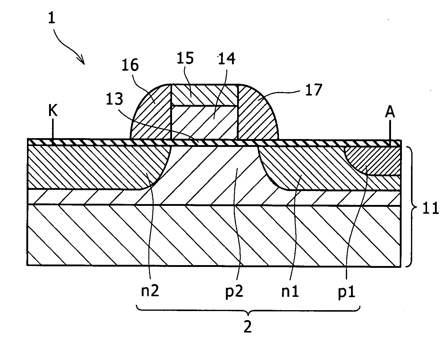
[0042]A semiconductor device according to one embodiment (first embodiment) of the present invention will be described below with reference to FIG. 1 as a sectional view of a schematic structure.

[0043]As shown in FIG. 1, a semiconductor device 1 includes a thyristor 2 arising from sequential joining of a first region (hereinafter, referred to as a first p-region) p1 of a first conductivity type (hereinafter, defined as the p-type), a second region (hereinafter, referred to as a first n-region) n1 of a second conductivity type (hereinafter, defined as the n-type) opposite to the first conductivity type, a third region (hereinafter, referred to as a second p-region) p2 of the first conductivity type (p-type), and a fourth region (hereinafter, referred to as a second n-region) n2 of the second conductivity type (n-type). Details of the semiconductor device 1 will be described below.

[0044]A germanium layer 12 is formed on a semiconductor substrate 11. In this germanium layer 12, the sec...

second embodiment

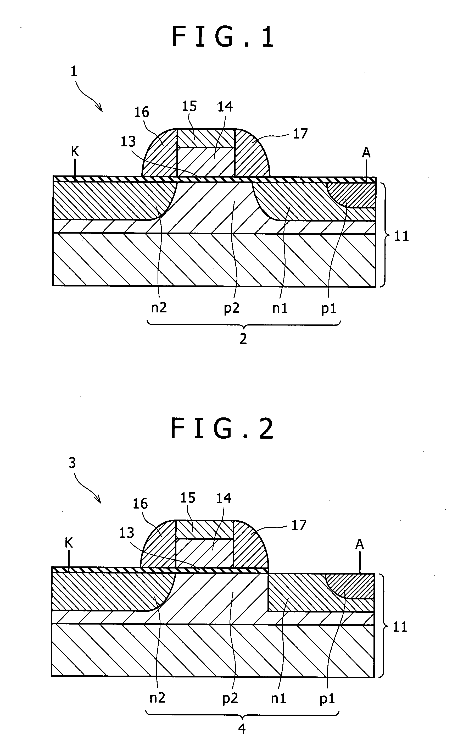
[0055]A semiconductor device according to one embodiment (second embodiment) of the present invention will be described below with reference to FIG. 2 as a sectional view of a schematic structure.

[0056]As shown in FIG. 2, a semiconductor device 3 includes a thyristor 4 arising from sequential joining of a first, region (hereinafter, referred to as a first p-region) p1 of a first conductivity type (hereinafter, defined as the p-type), a second region (hereinafter, referred to as a first n-region) n1 of a second conductivity type (hereinafter, defined as the n-type) opposite to the first conductivity type, a third region (hereinafter, referred to as a second p-region) p2 of the first conductivity type (p-type), and a fourth region (hereinafter, referred to as a second n-region) n2 of the second conductivity type (n-type). Details of the semiconductor device 3 will be described below.

[0057]In a semiconductor substrate 11, the second p-region p2 of the first conductivity type (p-type) i...

third embodiment

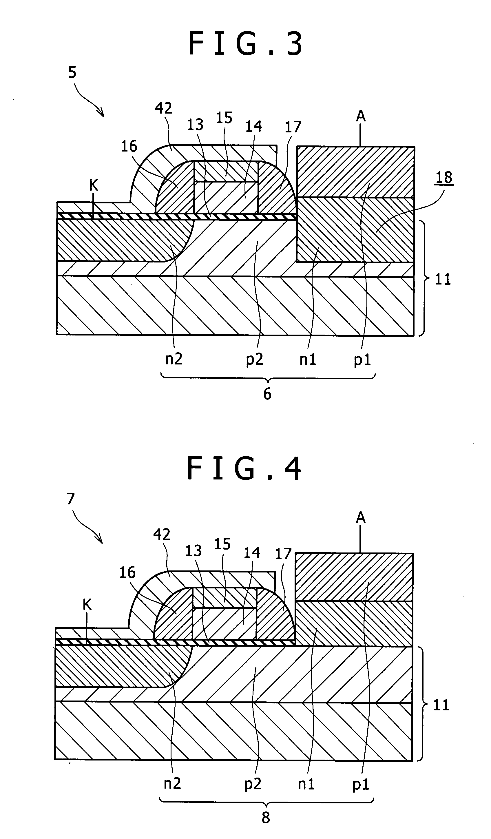
[0067]A semiconductor device according to one embodiment (third embodiment) of the present invention will be described below with reference to FIG. 3 as a sectional view of a schematic structure.

[0068]As shown in FIG. 3, a semiconductor device 5 includes a thyristor 6 arising from sequential joining of a first region (hereinafter, referred to as a first p-region) p1 of a first conductivity type (hereinafter, defined as the p-type), a second region (hereinafter, referred to as a first n-region) n1 of a second conductivity type (hereinafter, defined as the n-type) opposite to the first conductivity type, a third region (hereinafter, referred to as a second p-region) p2 of the first conductivity type (p-type), and a fourth region (hereinafter, referred to as a second n-region) n2 of the second conductivity type (n-type). Details of the semiconductor device 5 will be described below.

[0069]In a semiconductor substrate 11, the second p-region p2 of the first conductivity type (p-type) is ...


PUM


Abstract

A semiconductor device includes a thyristor configured to be formed through sequential joining of a first region of a first conductivity type, a second region of a second conductivity type opposite to the first conductivity type, a third region of the first conductivity type, and a fourth region of the second conductivity type, and have a gate formed over the third region. The first to fourth regions are formed in a silicon germanium region or germanium region.

Description

CROSS REFERENCES TO RELATED APPLICATIONS[0001]The present invention contains subject matter related to Japanese Patent Application JP 2006-210618 filed with the Japan Patent Office on Aug. 2, 2006, the entire contents of which being incorporated herein by reference.BACKGROUND OF THE INVENTION[0002]1. Field of the Invention[0003]The present invention relates to a semiconductor device having a thyristor and a method for manufacturing the semiconductor device.[0004]2. Description of the Related Art[0005]There has been proposed a memory (for an SRAM in particular) that employs a thyristor of which turn-on and turn-off characteristics are controlled by a gate electrode realized over the thyristor, and is connected in series to an access transistor (this memory will be referred to as a T-RAM, hereinafter). The memory operation thereof is realized in such a way that the off-region of the thyristor is defined as “0” and the on-region thereof as “1”.[0006]The thyristor is the combination of ...

Claims


Application Information

Patent Timeline
Patent Type & Authority Applications(United States)
IPC IPC(8): H01L29/74H01L21/332
CPCH01L27/0817H01L29/7455H01L29/7436H01L29/161
Inventor SUGIZAKI, TARO
Owner SONY CORP
Why Eureka
Try Eureka