
Connecting structure of printed circuit board of liquid crystal display module

a liquid crystal display module and flexible technology, applied in printed circuits, printed circuit aspects, electrical devices, etc., can solve the problems of hidden trouble of product yield, increased production cost, and high cost of the second flexible printed circuit board of the double-sided printed circuit board structure, so as to reduce the cost, improve the product yield, and insufficient bonding strength

Active Publication Date: 2008-02-21
WINTEK CORP
View PDF9 Cites 23 Cited by
  • Summary
  • Abstract
  • Description
  • Claims
  • Application Information

AI Technical Summary

Benefits of technology

[0015]In view of the above problems, the main objective of the present invention is to provide a connecting structure of the flexible printed circuit board of the LCD module, thereby lowering the cost and solving the problem of the false bonding and the insufficient bonding strength, so as to improve the product yield.
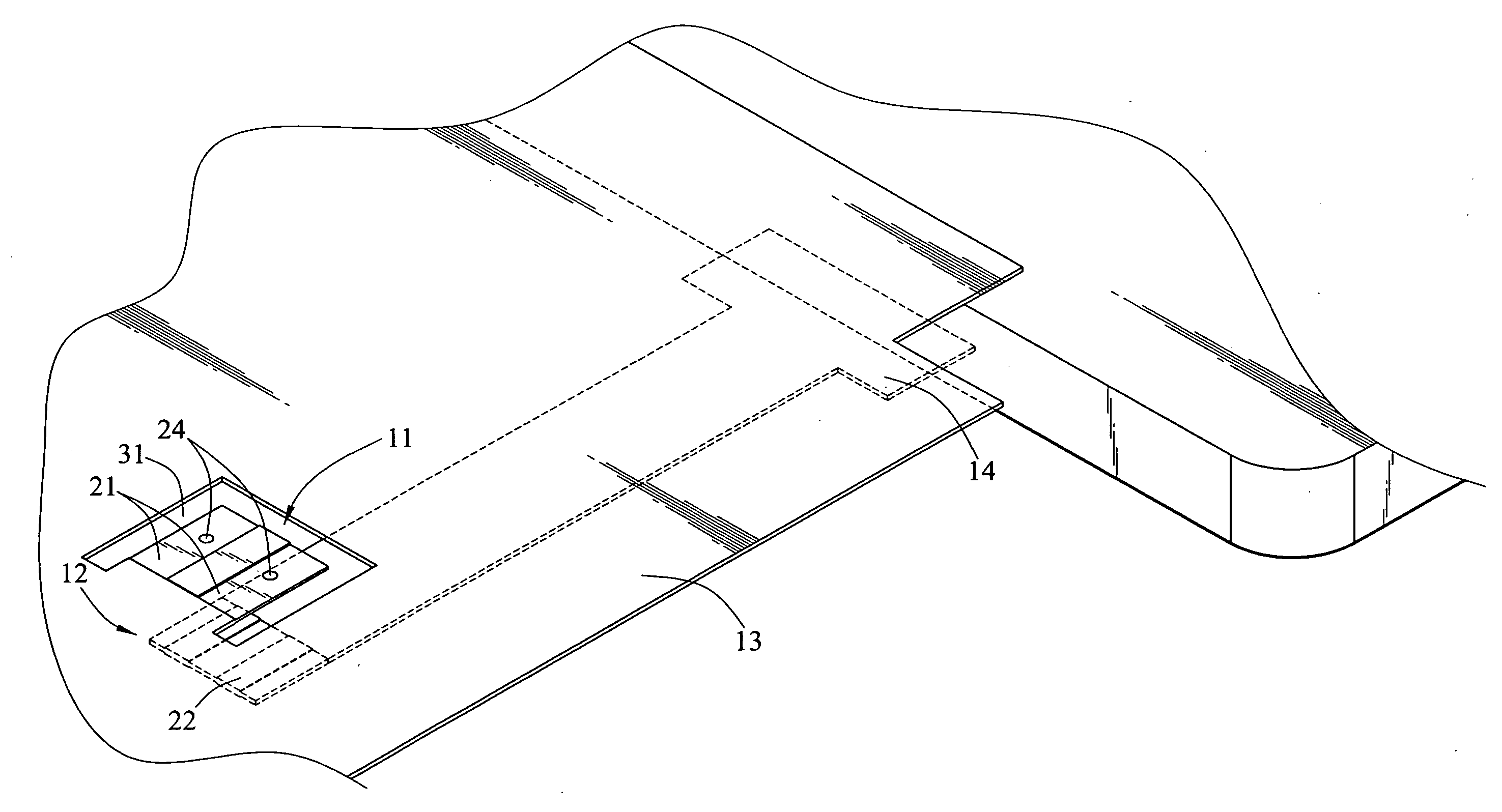
[0020]By the design of the connecting structure of the first flexible printed circuit board and the second flexible printed circuit board of the present invention, according to the structural requirement of the LCD module, the conducting surface of the second flexible printed circuit board may pass through the opening and select the corresponding solder surface of the first flexible printed circuit board to perform bonding, so as to facilitate the bonding operation, and improve the production performance. Moreover, by the effect of the PTHs, the solder may go deep into the PTHs of the first flexible printed circuit board and obtain the favorable tin feeding effect, so as to increase the bonding strength between the first flexible printed circuit board and the second flexible printed circuit board.

Problems solved by technology

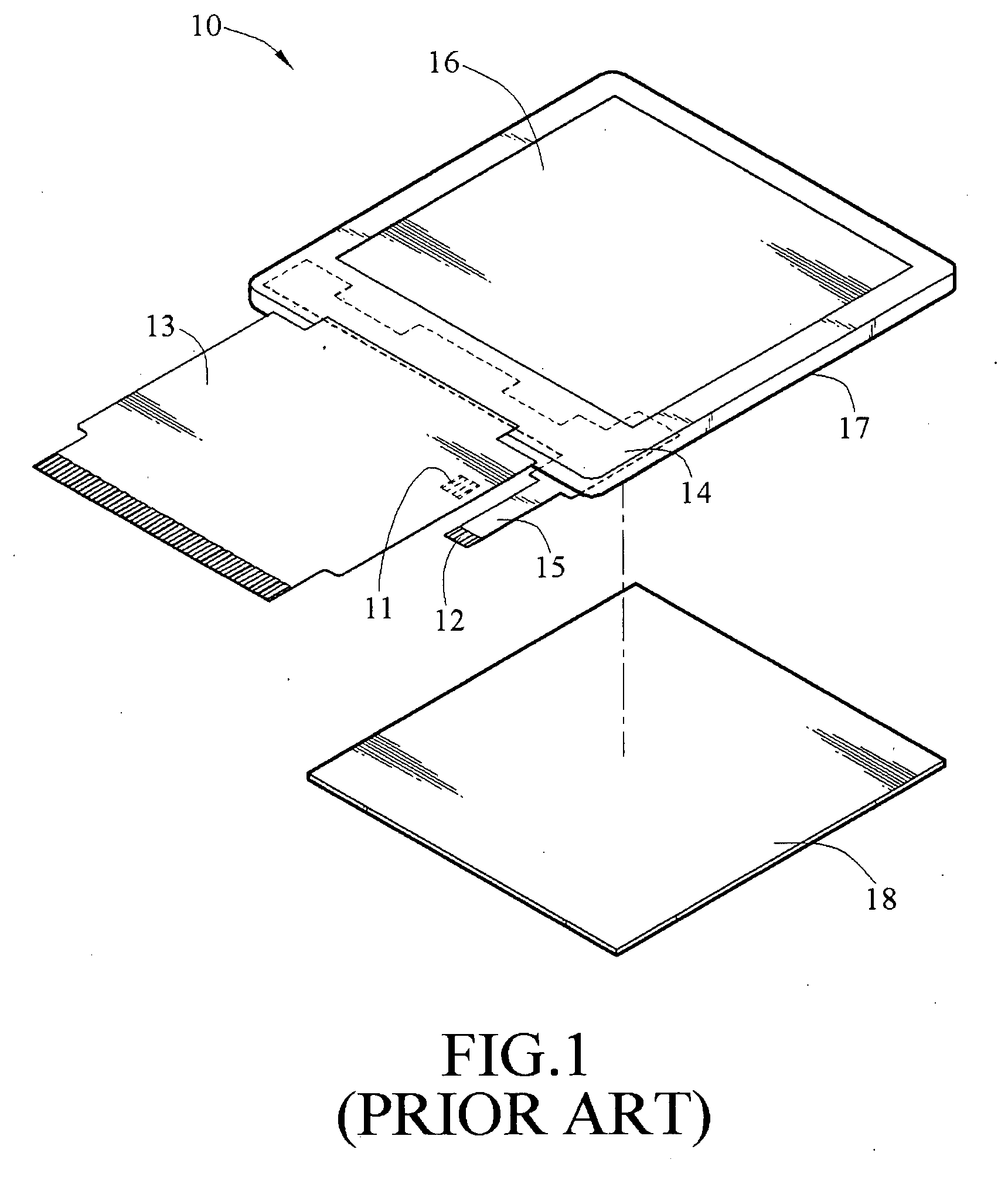
Although the above bonding structure is convenient for the bonding process, the second flexible printed circuit board of the double side printed circuit board structure is expensive, and the production cost is increased correspondingly.
However, whether the strength of the welding structure is appropriate becomes a hidden trouble of the product yield.
Usually, in order to make the welding structure have the substantive bonding strength, it is necessary to provide enough amount of solder, thus the tin bead is usually too big, causing the problems on the product assembling or the appearance dimension.
On the contrary, if the amount of the solder is not enough, the bonding section is too small, it is impossible to provide enough bonding strength, and the tin crack is easily generated because of the external force, thus resulting in the poor electrical connecting.
However, the heat energy must be transmitted though the protective layer of the flexible printed circuit board, usually the circuit board is burnt and becomes black.
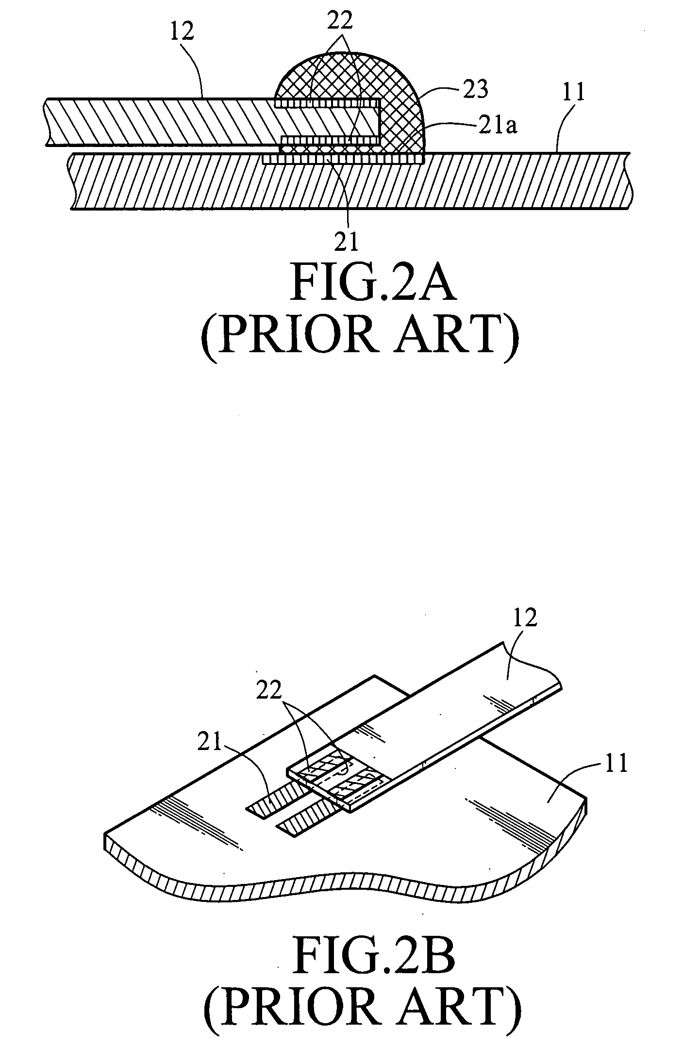
Because the solder 23 is located between the two pads, during the welding process, it is not easy to observe the melting condition of the solder 23, so usually the false bonding occurs, resulting in the poor electrical connecting, and thereby influencing the product yield.

Method used


Image

  • Connecting structure of printed circuit board of liquid crystal display module
  • Connecting structure of printed circuit board of liquid crystal display module
  • Connecting structure of printed circuit board of liquid crystal display module

Examples


Embodiment Construction

[0031]Referring to FIG. 5A, it is a schematic view of the first embodiment of the connecting structure of the flexible printed circuit board of the LCD module according to the present invention. As shown in FIG. 5A, the connecting structure of the flexible printed circuit board of the LCD module according to the present invention includes a first flexible printed circuit board 13 and a second flexible printed circuit board 14. The first flexible printed circuit board 13 is a double side printed circuit board structure, and the second flexible printed circuit board 14 is a single side printed circuit board structure. Both of the first flexible printed circuit board 13 and the second flexible printed circuit board 14 are flexible copper clad laminates. The first flexible printed circuit board 13 is a panel flexible printed circuit board connected to the LCD panel and the mainboard printed circuit board (not shown), so as to finish the signal transmission. The second flexible printed c...


PUM


Abstract

A connecting structure of a printed circuit board of a liquid crystal display (LCD) module includes a double side printed circuit board and a single side printed circuit board. With the design of the double side printed circuit board having a solder element with two solder surfaces with a plurality of plated through holes (PTHs), and the design of the opening neighboring the solder element, the conducting surface of the single side printed circuit board may easily accord with the structural requirements to select the corresponding solder surface for performing welding.

Description

CROSS-REFERENCE TO RELATED APPLICATIONS[0001]This non-provisional application claims priority under 35 U.S.C. §119(a) on Patent Application No(s). 095130499 filed in Taiwan, R.O.C. on Aug. 18, 2006, the entire contents of which are hereby incorporated by reference.BACKGROUND OF THE INVENTION[0002]1. Field of Invention[0003]The present invention relates to a connecting structure of a printed circuit board. More particularly, the present invention relates to a connecting structure of a flexible printed circuit board of a liquid crystal display (LCD) module.[0004]2. Related Art[0005]Recently, because the objectives of the electronic products are light, thin, short and small, many electronic devices develop according to the objectives, and the using of the flexible printed circuit board totally accord with the requirement of the modern technology. In addition, due to the unique flexibility of the flexible printed circuit board, the three-dimensional stereo wiring may be easily accomplis...

Claims


Application Information

Patent Timeline
IPC IPC(8): H01R12/24
CPCH01R4/027H05K1/147H05K3/363H01R12/7076H05K2201/058H05K2201/09081H05K2201/048H01R12/00
Inventor CHOU, YUNG-WEI
Owner WINTEK CORP
Learn More