Method for hermetically sealing an OLED display
- Summary
- Abstract
- Description
- Claims
- Application Information
AI Technical Summary
Benefits of technology
Problems solved by technology
Method used
Image

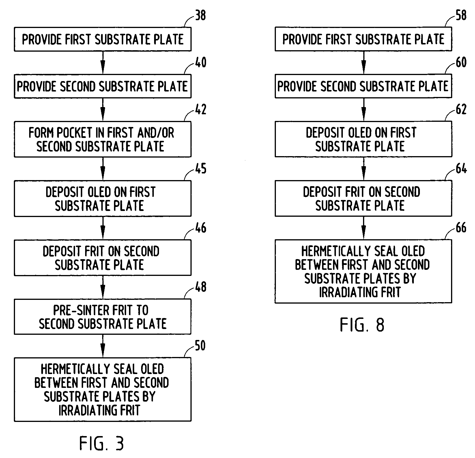
Examples
Embodiment Construction
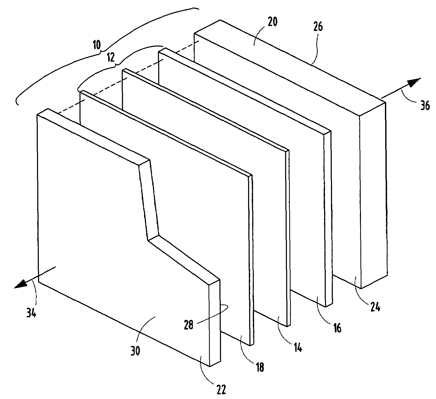
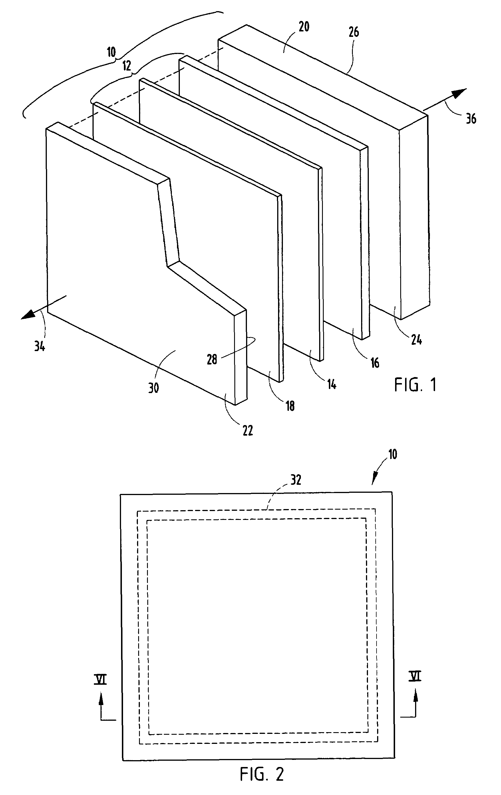
[0021]For purposes of description herein, the terms “upper,”“lower,”“right,”“left,”“rear,”“front,”“vertical,”“horizontal,” and derivatives thereof shall relate to the invention as oriented in FIGS. 1 and 3. However, it is to be understood that the invention may assume various alternative orientations and step sequences, except where expressly specified to the contrary. It is also to be understood that the specific devices and processes illustrated in the attached drawings, and described in the following specification are exemplary embodiments of the inventive concepts defined in the appended claims. Hence, specific dimensions and other physical characteristics relating to the embodiments disclosed herein are not to be considered as limiting, unless the claims expressly state otherwise.
[0022]Reference numeral 10 (FIG. 1) generally designates a top emission, organic light-emitting diode display embodying the present invention. The display 10 comprises an organic light-emitting diode 1...
PUM
 Abstract
Description
Claims
Application Information
 - R&D Engineer
- R&D Manager
- IP Professional
- Industry Leading Data Capabilities
- Powerful AI technology
- Patent DNA Extraction
Browse by: Latest US Patents, China's latest patents, Technical Efficacy Thesaurus, Application Domain, Technology Topic.
© 2024 PatSnap. All rights reserved.Legal|Privacy policy|Modern Slavery Act Transparency Statement|Sitemap