Semiconductor integrated circuit and testing method of same

a technology of integrated circuits and semiconductors, applied in the direction of testing circuits, semiconductor/solid-state device testing/measurement, instruments, etc., can solve the problems of long analysis time, inability to identify good and bad chips, and the failure of most circuits in bad chips normally operating, etc., to achieve easy identification, easy detection, and easy testing

Inactive Publication Date: 2008-02-28
SOCIONEXT INC
View PDF8 Cites 14 Cited by
  • Summary
  • Abstract
  • Description
  • Claims
  • Application Information

AI Technical Summary

Benefits of technology

[0010]An object of the present invention is to easily identify whether a semiconductor integrated circuit is a good product or not.
[0011]In one aspect of the present invention, a program circuit activates a pass signal when a first program unit is programmed. The first program unit is programmed when a test of an internal circuit is passed. A mode setting circuit switches an operation mode to a normal operation mode or a test mode by external control. A state machine allows a partial circuit of the internal circuit to perform an unusual operation different from a normal operation when the pass signal is inactivated during the normal operation mode. Here, the unusual operation is an operation recognizable from outside a semiconductor integrated circuit. By recognizing the unusual operation in the normal operation mode, it can be easily recognized that the semiconductor integrated circuit is bad. Since a failure can be recognized without shifting to the test mode, for example, a user who purchases the semiconductor integrated circuit can also easily recognize the failure.
[0012]Further, the state machine disables the unusual operation of the partial circuit and allows it to perform the normal operation during the test mode or when the pass signal is activated. During the test mode, the unusual operation is disabled regardless of a program state of the first program unit. Therefore, for example, a maker of the semiconductor integrated circuit can easily perform a test of the semiconductor integrated circuit by switching the operation mode from the normal operation mode to the test mode in a test process even when the first program unit is not programmed. Then, in a programming process, only in the semiconductor integrated circuit which has passed the test, the first program unit is programmed.

Problems solved by technology

However, if the position of the ink mark is shifted by one chip, the ink mark becomes faint, or a wrong failure map file is created due to a problem in the manufacturing process, a user who has purchased the wafer may be unable to identify the good and bad chips.
Further, when a chip which caused the above problem is returned from the user to a semiconductor maker, a long time is sometimes needed to analyze a failure.
Programming the fuse of the bad chip or the good chip is performed to identify the good chip or the bad chip in the manufacturing process of the semiconductor integrated circuit, but does not give consideration to the user who purchases the semiconductor integrated circuit.
Further, for example, if only one memory cell is bad in the bad chip, most circuits in the bad chip normally operate.
Therefore, it is difficult for the user to identify the good and bad chips in the state where the wrong ink mark is put or the wrong failure map file is created.
In particular, in the wafer shipment in which the bad chip is mixed, after a product in which the chip is mounted is assembled by the user, the failure in the chip is sometimes revealed in a test process of the product.
Hence, it is difficult for the user to identify whether the chip is shipped as the good chip.
By recognizing the unusual operation in the normal operation mode, it can be easily recognized that the semiconductor integrated circuit is bad.

Method used


Image

  • Semiconductor integrated circuit and testing method of same
  • Semiconductor integrated circuit and testing method of same
  • Semiconductor integrated circuit and testing method of same

Examples


first embodiment

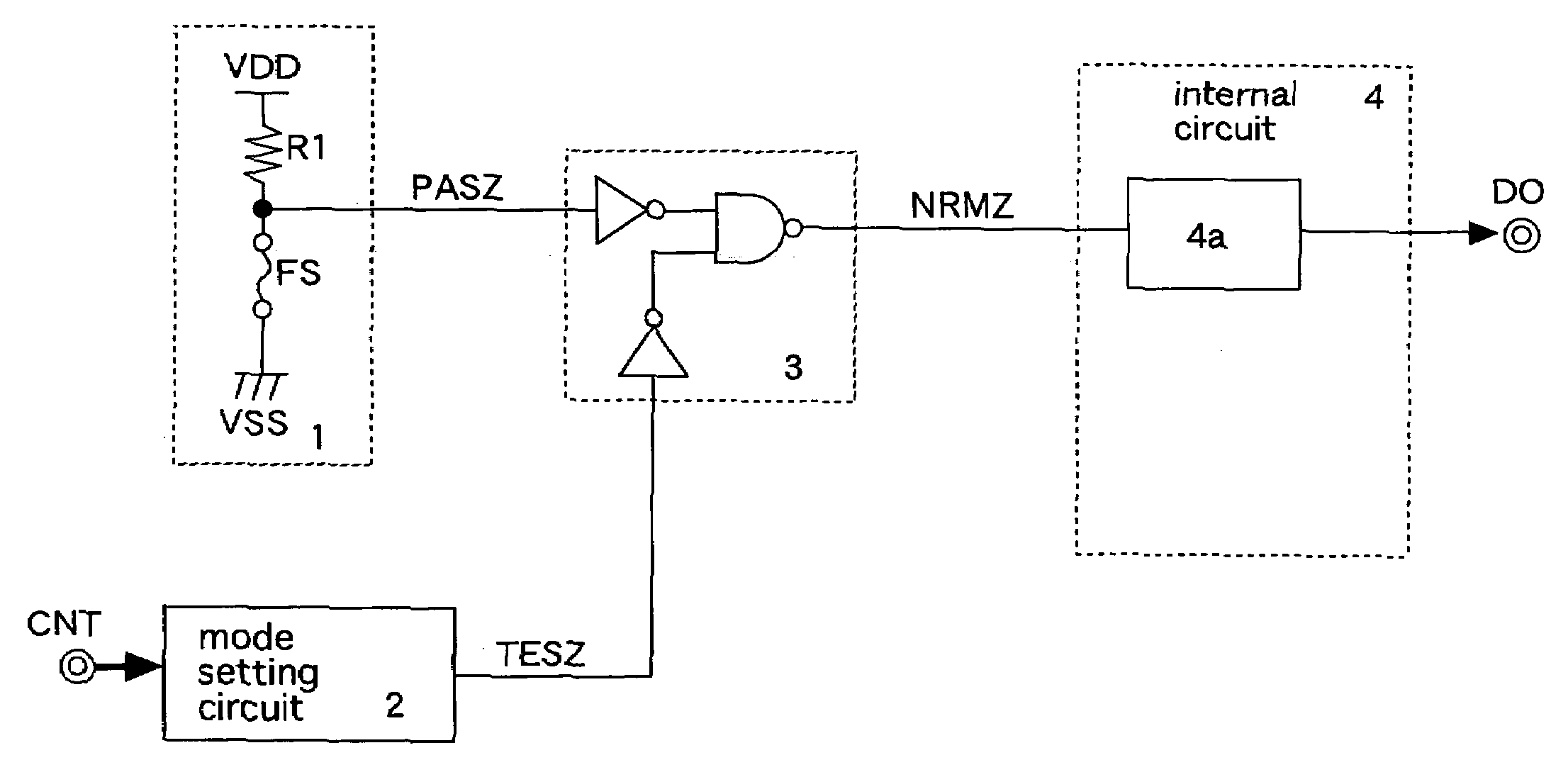
[0028]FIG. 1 shows the present invention. A semiconductor integrated circuit includes a program circuit 1, a mode setting circuit 2, a state machine 3, and an internal circuit 4. The program circuit 1 includes a resistor R1 and a fuse FS (first program unit) connected in series between a power supply line VDD and a ground line VSS. The fuse FS is programmed (cut) when a test of the internal circuit 4 is passed. For example, the fuse FS is a fuse programmed by irradiation of a laser beam. Alternatively, the fuse FS is a fuse programmed by an overvoltage or an overcurrent. Further, the fuse FS may be constituted using an electrically programmable nonvolatile memory cell.

[0029]The program circuit 1 activates a pass signal PASZ outputted from a connection node between the resistor R1 and the fuse FS to a high logic level when the fuse FS is programmed. The program circuit 1 inactivates the pass signal PASZ to a low logic level when the fuse FS is not programmed. As will be described in ...

second embodiment

[0041]FIG. 5 shows the present invention. A semiconductor integrated circuit of this embodiment is, for example, an FCRAM (Fast Cycle RAM) including DRAM memory cells and including an SRAM interface. The FCRAM includes a command decoder 10, a mode register 12 (mode setting circuit), a program circuit 14, an address input circuit 16, a data input / output circuit 18, a state machine 20, a core control circuit 22, a redundancy fuse circuit 24, an address comparison circuit 26, and a memory core 28. Further, the FCRAM includes a refresh timer, a refresh address counter, and so on, which are not shown, to automatically perform a refresh operation. Since the present invention does not relate to control of the refresh operation of a memory cell, circuits and operations related to the refresh operation will not be described.

[0042]The command decoder 10 outputs commands CMD recognized according to the logic levels of a chip enable signal / CE1, a write enable signal / WE, and an output enable s...

fifth embodiment

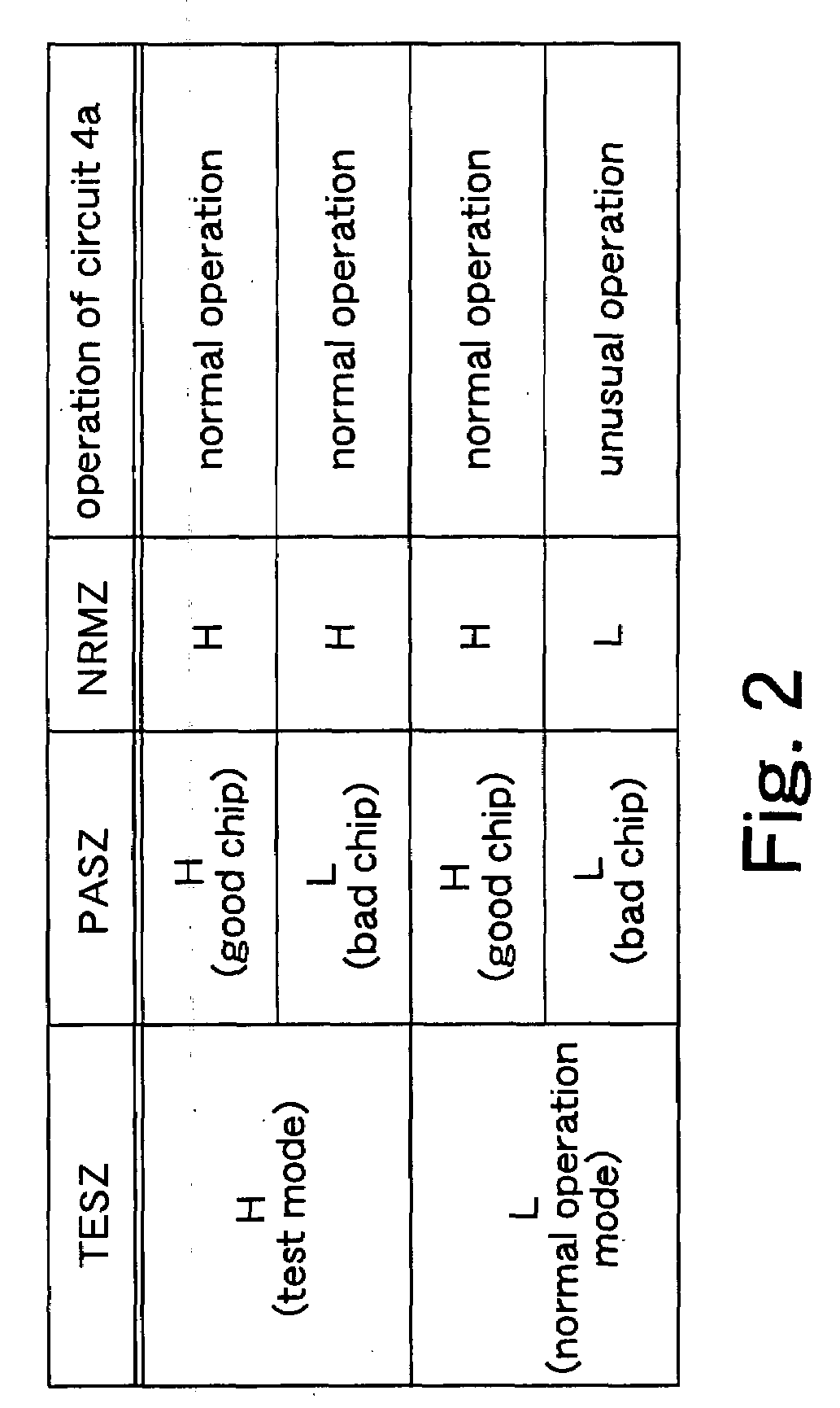
[0082]In the above fifth embodiment, the example in which the output of data is disabled when the normal signal NRMZ is inactivated is described. The present invention is not limited to this embodiment. For example, when the normal signal NRMZ is inactivated, data fixed to a high logic level may be outputted or data fixed to a low logic level may be outputted.


PUM


Abstract

A program circuit activates a pass signal when a first program unit is programmed. The first program unit is programmed when a test of an internal circuit is passed. A mode setting circuit switches an operation mode to a normal operation mode or a test mode by external control. A state machine allows a partial circuit of the internal circuit to perform an unusual operation different from a normal operation when the pass signal is inactivated during the normal operation mode. By recognizing the unusual operation during the normal operation mode, it can be easily recognized that a semiconductor integrated circuit is bad. Since a failure can be recognized without shifting to the test mode, for example, a user who purchases the semiconductor integrated circuit can also easily recognize the failure.

Description

CROSS REFERENCE TO RELATED APPLICATION[0001]This application is based upon and claims the benefit of priority from Japanese Patent Application No. 2006-229578, filed on Aug. 25, 2006, the entire contents of which are incorporated herein by reference.BACKGROUND[0002]1. Field[0003]The present invention relates to a semiconductor integrated circuit including a program circuit of a fuse or the like and a testing method of the same.[0004]2. Description of the Related Art[0005]Generally, after being manufactured, a semiconductor integrated circuit (hereinafter also referred to a chip) is tested and classified as a good chip or a bad chip. A technique of programming a fuse of a bad chip to electrically identify the good chip or the bad chip in a manufacturing process is proposed (for example, Japanese Unexamined Patent Application Publication No. Hei 7-30068, Japanese Unexamined Patent Application Publication No. Hei 11-243124, Japanese Unexamined Patent Application Publication No. Hei 3-2...

Claims


Application Information

Patent Timeline
Patent Type & Authority Applications(United States)
IPC IPC(8): G01R31/26G01R31/28G11C29/44H01L21/66
CPCG11C29/006G11C2029/4402G11C29/46G11C29/44G11C29/00H01L27/04
Inventor YAMAGUCHI, KOTA
Owner SOCIONEXT INC
Why Eureka
Try Eureka