Inductor element and integrated electronic component

a technology of electronic components and inductor elements, applied in the direction of basic electric elements, fixed transformers or mutual inductances, inductances, etc., can solve the problems of inhibiting the increase of q value, inducing significant parasitic capacitance of inductor, and disadvantageous inductance for increasing q value, etc., to achieve the effect of achieving a higher q valu

Inactive Publication Date: 2008-02-28
FUJITSU LTD
View PDF8 Cites 26 Cited by
  • Summary
  • Abstract
  • Description
  • Claims
  • Application Information

AI Technical Summary

Benefits of technology

[0012]The present invention has been proposed in view of the foregoing situation, with an object to provi

Problems solved by technology

Besides, in the case where the inductor is constituted of a plurality of spiral coils stacked in multiple layers (multilayer inductor) in the multilayer ceramic substrate in the IPD manufactured through the LTCC process, the inductor incurs significant parasitic capacitance because of the presence of the ceramic material (dielectric material) between the mutually adjacent portions of

Method used


Image

  • Inductor element and integrated electronic component
  • Inductor element and integrated electronic component
  • Inductor element and integrated electronic component

Examples


first embodiment

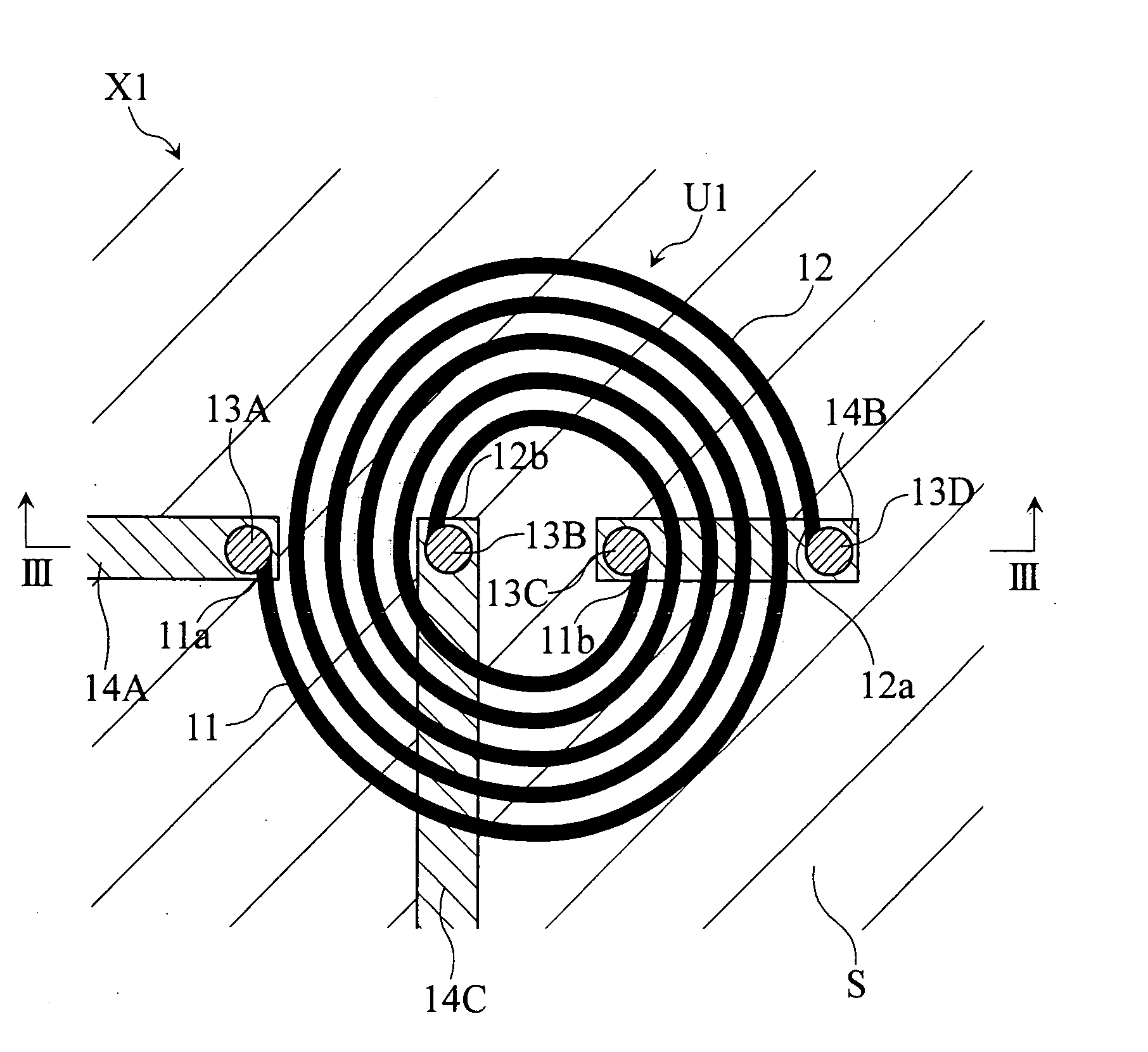
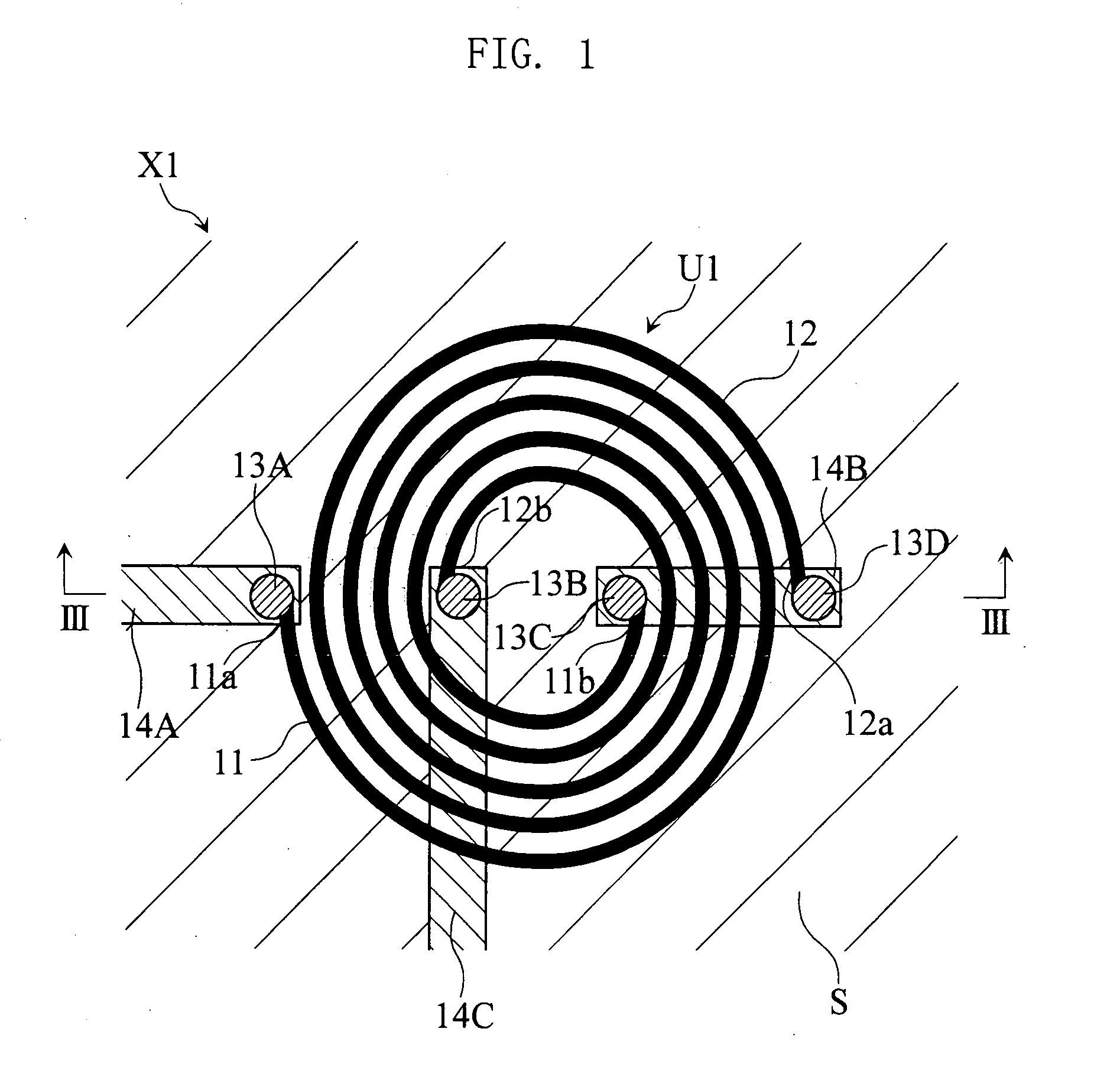
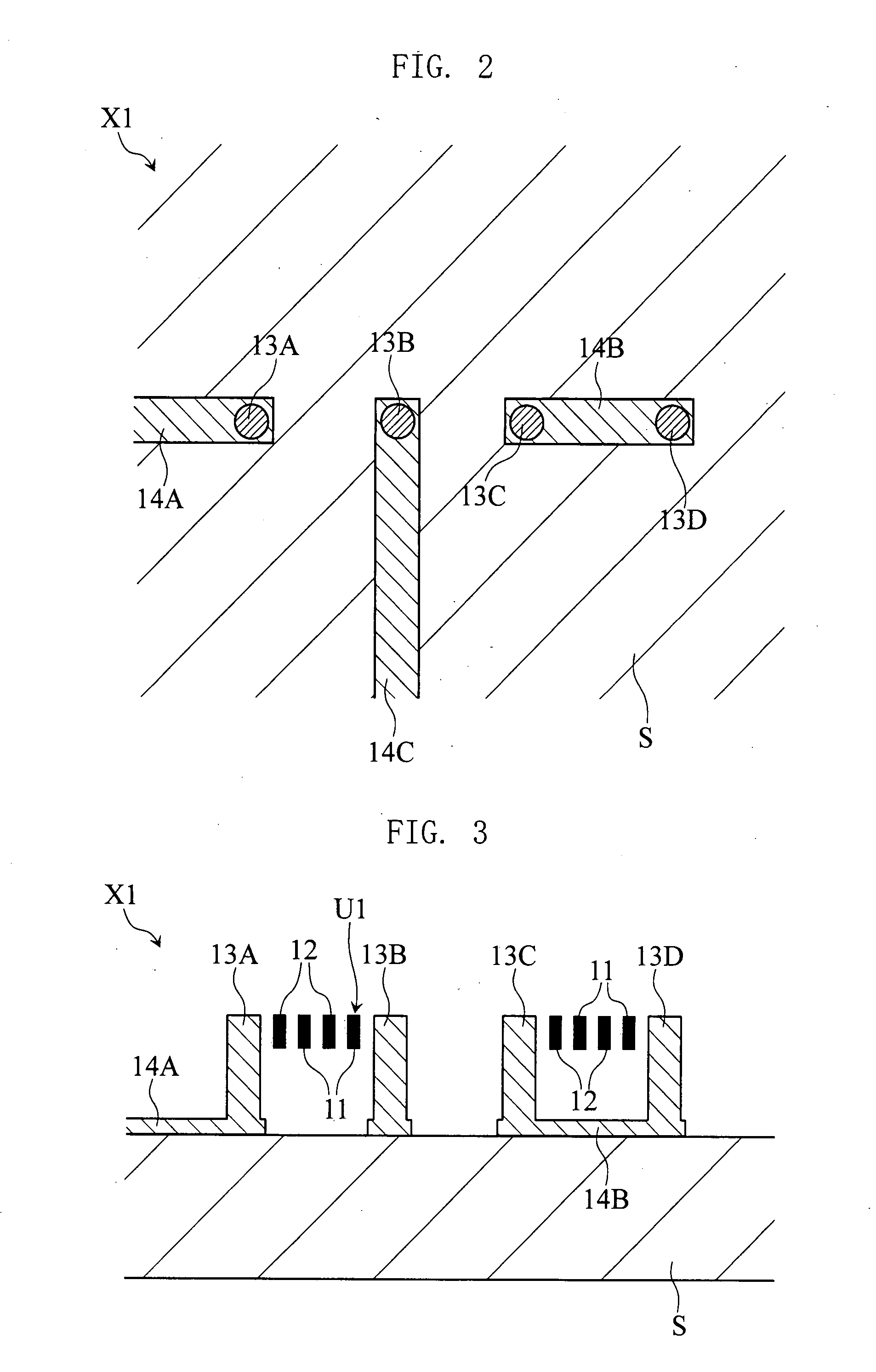
[0066]FIGS. 1 to 3 illustrate an inductor element X1 according to the present invention. FIG. 1 is a plan view of the inductor element X1. FIG. 2 is a fragmentary plan view of the inductor element X1. FIG. 3 is a cross-sectional view taken along a line III-III in FIG. 1.

[0067]The inductor element X1 includes a substrate S, a coil unit U1 (not shown in FIG. 2), conductive columns 13A, 13B, 13C, 13D, and interconnects 14A, 14B, 14C.

[0068]The substrate S may be a semiconductor substrate (for example constituted of a silicon material, such as monocrystalline silicon), a quartz substrate, a glass substrate, a ceramic substrate, a silicon-on-insulator (SOI) substrate, a silicon-on-quartz (SOQ) substrate, or a silicon-on-glass (SOG) substrate, and a surface thereof is coated with a dielectric material, as may be required. At least the outermost layer of the substrate S includes the dielectric material.

[0069]The coil unit U1 includes two spiral coils 11, 12 located with a spacing from the s...

second embodiment

[0076]FIGS. 4 to 7 illustrate an integrated electronic component Yl according to the present invention. FIG. 4 is a plan view of the integrated electronic component Y1. FIG. 5 is a fragmentary plan view of the integrated electronic component Y1. FIGS. 6 and 7 are cross-sectional views taken along a line VI-VI and VII-VII in FIG. 4, respectively.

[0077]The integrated electronic component Y1 includes a substrate S, a coil unit U2 (not shown in FIG. 5), a coil unit U3, conductive columns 25A, 25B, 25C, 25D, a capacitor 26, pads 27A, 27B, 27C, 27D, and interconnects 28A, 28B, 28C, 28D, and may be expressed as the circuit diagram shown in FIG. 8.

[0078]The coil unit U2 includes two spiral coils 21, 22 located with a spacing from the substrate S. As shown in FIG. 4, the spiral coil 21 includes a spiral-shaped coil lead, with an outer end portion 21a and an inner end portion 21b. The spiral coil 22 includes a spiral-shaped coil lead, with an outer end portion 22a and an inner end portion 22b...

third embodiment

[0087]FIGS. 10 to 13 illustrate an integrated electronic component Y2 according to the present invention. FIG. 10 is a plan view of the integrated electronic component Y2. FIG. 11 is a fragmentary plan view of the integrated electronic component Y2. FIGS. 12 and 13 are cross-sectional views taken along a line XII-XII and XIII-XIII in FIG. 10, respectively.

[0088]The integrated electronic component Y2 includes a substrate S, a coil unit U4 (not shown in FIG. 11), a coil unit U5, conductive columns 35A, 35B, 35C, 35D, a capacitor 36, pads 37A, 37B, 37C, 37D, and interconnects 38A, 38B, 38C, and may be expressed as the circuit diagram shown in FIG. 14.

[0089]The coil unit U4 includes two spiral coils 31, 32 located with a spacing from the substrate S. As shown in FIG. 10, the spiral coil 31 includes a spiral-shaped coil lead, with an outer end portion 31a and an inner end portion 31b. The spiral coil 32 includes a spiral-shaped coil lead, with an outer end portion 32a and an inner end po...


PUM


Abstract

An inductor element and an integrated electronic component that facilitate achieving a higher Q value are provided. The inductor element includes a substrate, a coil unit spaced from the substrate, and a plurality of conductive columns. The coil unit includes a plurality of spiral coils each constituted of a spiral-shaped coil lead. The spiral coils are disposed such that their winding directions are the same, and that the coil lead of each spiral coil includes a portion extending between the coil lead of at least one of the other spiral coils. End portions of the spiral coils are fixed to the substrate via the conductive columns. The integrated electronic component of the invention includes such inductor element.

Description

BACKGROUND OF THE INVENTION[0001]1. Field of the Invention[0002]The present invention relates to an inductor element, and to an integrated electronic component including an inductor element as a part.[0003]2. Description of the Related Art[0004]A RF (radio frequency) system or a RF circuit employed in a mobile phone or the like generally includes an integrated passive device (hereinafter, IPD) as a high-frequency module device, for upgrading the performance and reducing the dimensions and weight. In the IPD, passive components such as an inductor, a capacitor, a resistor, and a filter required according to the design are integrated, among which the inductor rarely fails to be incorporated. The inductor generally has a relatively low Q value, for example in comparison with the capacitor, and hence incorporating the inductor in the IPD often degrades the Q value thereof as a whole. Accordingly, various studies are being pursued for achieving a higher Q value of the IPD that includes t...

Claims


Application Information

Patent Timeline
IPC IPC(8): H01F5/00
CPCH03H2001/0092H01F19/04H01F2017/0086
Inventor MATSUMOTO, TSUYOSHIMI, XIAOYUMIZUNO, YOSHIHIRO
Owner FUJITSU LTD
Why Eureka
Try Eureka