Josephson device, method of forming Josephson device and superconductor circuit

a superconductor circuit and a technology of josephson devices, applied in the direction of superconductors/hyperconductors, semiconductor devices, semiconductor/solid-state device details, etc., can solve the problems of not being able to obtain a sufficiently large icrn product, only forming bi-crystal-type junctions, and unsuitable for high-performance devices that require complex structures. , to achieve the effect of suppressing current leakage, avoiding damag

Active Publication Date: 2008-02-28
THE CHUGOKU ELECTRIC POWER CO INC +1
View PDF1 Cites 10 Cited by
  • Summary
  • Abstract
  • Description
  • Claims
  • Application Information

AI Technical Summary

Benefits of technology

[0012]Still another object of the present invention is to provide a Josephson device comprising a first superconducting electrode layer, a barrier layer and a second superconducting electrode layer that are successively stacked, wherein the first and second superconducting electrode layers are made of an oxide superconductor material having (RE)1(AE)2Cu3Oy as a main component, where an element RE is at least one element selected from a group consisting of Y, La, Pr, Nd, Sm, Eu, Gd, Dy, Ho, Er, Tm, Yb and Lu, and an element AE is at least one element selected from a group consisting of Ba, Sr and Ca, and the barrier layer is made of a material that includes the element RE, the element AE, Cu and oxygen, where in cations within the material forming the barrier layer, a Cu content is in a range of 35 At. % to 55 At. % and an RE content is in a range of 12 At. % to 30 At. %, and the barrier layer has a composition different from compositions of the first and second superconducting electrode layers. According to the present invention, it is possible to avoid the problem of the Cu content of the barrier layer becoming extremely small, unlike the conventional IEJ, because the barrier layer is a deposited layer of the oxide material, and a satisfactory superconducting junction can be formed. As a result, it is possible to improve the IcRn product of the Josephson device. In addition, it is also possible to suppress inconsistencies in the critical current value Ic. Moreover, the critical temperature of the superconducting junction becomes high compared to that of the conventional IEJ. Consequently, the cooling cost of the Josephson device can be reduced. It is preferable that the compositions of the first and second superconducting electrode layers are detected by an analyzing method similar to that used to detect the composition of the barrier layer, and to compare the compositions at a distance of approximately 10 nm from the interface between the barrier layer and the first and second superconducting electrode layers.
[0014]Another object of the present invention is to provide a Josephson device comprising a substrate having a surface; a first superconducting electrode layer formed on the surface of the substrate; an insulator formed on the first superconducting electrode layer and having a penetration hole penetrating the insulator layer in a direction taken along a thickness of the insulator layer; a barrier layer deposited on the first superconducting electrode layer and within the penetration hole; and a second superconducting electrode layer filling the penetration hole and covering the barrier layer and the insulator layer, wherein the first and second superconducting electrode layers are made of an oxide superconductor material having (RE)1(AE)2Cu3Oy as a main component, where an element RE is at least one element selected from a group consisting of Y, La, Pr, Nd, Sm, Eu, Gd, Dy, Ho, Er, Tm, Yb and Lu, and an element AE is at least one element selected from a group consisting of Ba, Sr and Ca; and the barrier layer is made of a material that includes the element RE, the element AE, Cu and oxygen, where in cations within the material forming the barrier layer, a Cu content is in a range of 35 At. % to 55 At. % and an RE content is in a range of 12 At. % to 30 At. %, and the barrier layer has a composition different from compositions of the first and second superconducting electrode layers. According to the present invention, it is possible to realize a stacked type Josephson device that can obtain effects similar to those described above.
[0015]Still another object of the present invention is to provide a method of forming a Josephson device comprising the steps of (a) forming on a substrate a first superconducting electrode layer made of an oxide superconductor material; (b) forming an insulator layer covering the first superconducting electrode layer; (c) removing a portion of the insulator layer to expose the first superconducting electrode layer; (d) depositing a barrier layer made of an oxide material on an exposed surface of the first superconducting electrode layer; and (e) forming a second superconducting electrode layer made of an oxide superconductor material to cover the barrier layer, wherein the oxide material forming the barrier layer includes an element RE, an element AE, Cu and oxygen, where the element RE is at least one element selected from a group consisting of Y, La, Pr, Nd, Sm, Eu, Gd, Dy, Ho, Er, Tm, Yb and Lu, and the element AE is at least one element selected from a group consisting of Ba, Sr and Ca. According to the present invention, because the barrier layer is a deposited layer, the layer quality of the barrier layer becomes satisfactory compared to that of the barrier layer of the conventional IEJ, and the IcRn product is improved. It is possible to avoid damages within the crystals and to suppress the current leak, even if the Cu content of the barrier layer is high such that the current leak would otherwise be generated between the first and second superconductor electrode layers of the Josephson device using the conventional IEJ.
[0016]A further object of the present invention is to provide a superconductor circuit using magnetic flux quantum as signal carrier, comprising at least one Josephson device comprising a first superconducting electrode layer, a barrier layer and a second superconducting electrode layer that are successively stacked, wherein the first and second superconducting electrode layers are made of an oxide superconductor material having (RE)1(AE)2Cu3Oy as a main component, where an element RE is at least one element selected from a group consisting of Y, La, Pr, Nd, Sm, Eu, Gd, Dy, Ho, Er, Tm, Yb and Lu, and an element AE is at least one element selected from a group consisting of Ba, Sr and Ca; and the barrier layer is made of a material that includes the element RE, the element AE, Cu and oxygen, where in cations within the material forming the barrier layer, a Cu content is in a range of 35 At. % to 55 At. % and an RE content is in a range of 12 At. % to 30 At. %, and the barrier layer has a composition different from compositions of the first and second superconducting electrode layers. According to the present invention, it is possible to realize a superconductor circuit having the Josephson device that can obtain effects similar to those described above.

Problems solved by technology

However, the bi-crystal type junction can only be formed at the bonding interface of the substrate, and is unsuited for application to high-performance devices that require complex structures.
The IcRn product must be large in order to realize such a Josephson device, but a sufficiently large IcRn product has not be obtained in T. Satoh et al. and Y. Soutome et al. referred above.

Method used


Image

  • Josephson device, method of forming Josephson device and superconductor circuit
  • Josephson device, method of forming Josephson device and superconductor circuit
  • Josephson device, method of forming Josephson device and superconductor circuit

Examples


first embodiment

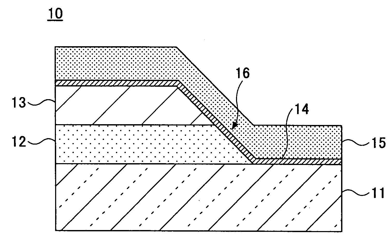
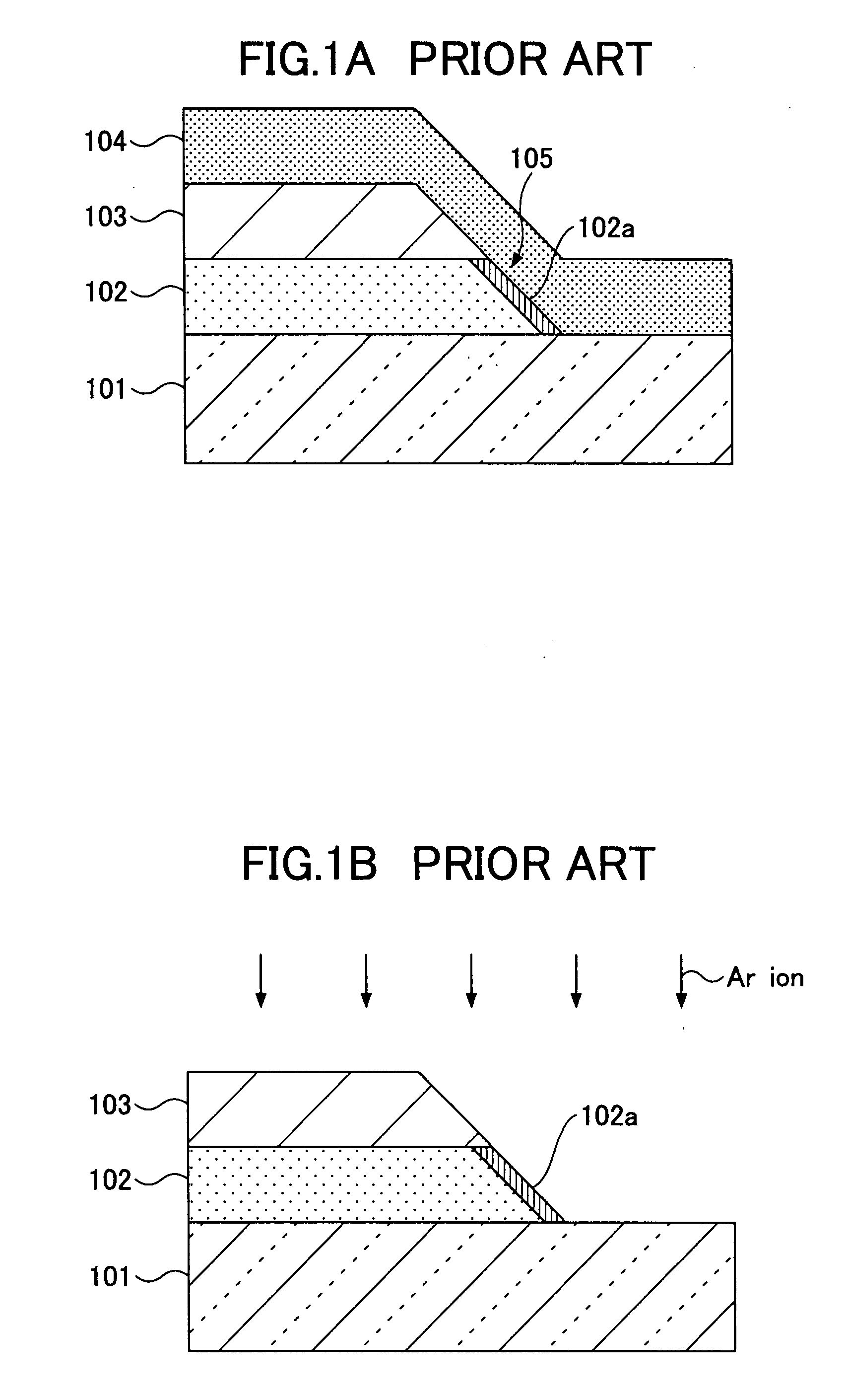
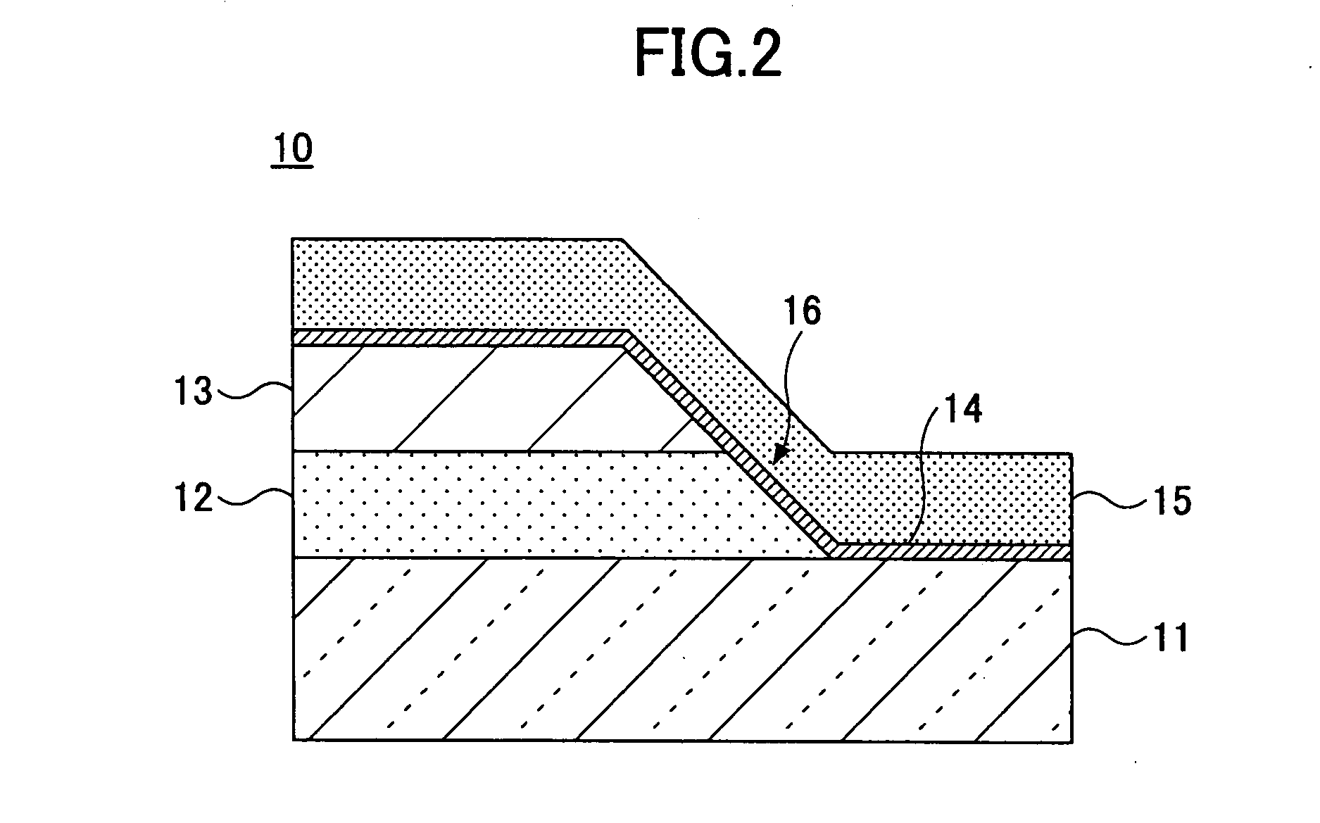
[0038]FIG. 2 is a cross sectional view showing a Josephson device in a first embodiment of the present invention.

[0039]A Josephson device 10 of the first embodiment shown in FIG. 2 has the ramp-edge structure. The Josephson device 10 has a substrate 11, a lower electrode layer 12 formed on the substrate 11, an insulator layer 13 covering the lower electrode layer 12, a barrier layer 14, and an upper electrode layer 15 covering the barrier layer 14. The barrier layer 14 covers a surface of the substrate 11, a sloping surface formed at one end of each of the lower electrode layer 12 and the insulator layer 13, and a surface of the insulator layer 13. A superconducting junction 16 is formed by the lower electrode layer 12, the barrier layer 14 and the upper electrode layer 15.

[0040]The substrate 11 is made of a material having a crystal structure that allows epitaxial growth of the lower electrode layer 12 on the substrate 11. For example, the substrate 11 may be made of a material sel...

embodiment sample emb1-1

[0072]Embodiment samples Emb1-1 were formed to have the same structure as the Josephson device 10 shown in FIG. 2 including the barrier layer 14 formed by the ramp-edge type deposition layer.

[0073]First, a YBa2Cu3Oy layer was formed, as a lower electrode layer, on a MgO substrate to a thickness of 200 nm by magnetron sputtering using a YBa2Cu3Oy target, at a substrate temperature of 740° C., an Ar+10 Vol. % O2 atmosphere, and a pressure of 80 mTorr, where Vol. % denotes volume percent. Then, a SrSnO3 layer was formed, as an insulator layer, on the lower electrode layer to a thickness of 250 nm by magnetron sputtering using a SrSnO3 target, at a substrate temperature of 680° C., an Ar+50 Vol. % O2 atmosphere, and a pressure of 50 mTorr.

[0074]Thereafter, the lower electrode layer and the insulator were etched by Ar ions using as a mask a resist layer having an opening formed by photolithography in a region where a superconducting junction is to be formed, so as to form a sloping surfa...

embodiment sample emb1-2

[0093]Embodiment samples Emb1-2 were formed using targets having the same compositions as those used when forming the embodiment samples Emb1-1, except for the barrier layer and the upper electrode layer, so as to obtain Josephson devices including a ramp-edge type barrier layer that is a deposited layer.

[0094]The barrier layer was formed on the substrate, the sloping surface portion of the lower electrode layer, and the sloping surface portion and the surface of the insulator layer to a thickness of 1.5 nm by PLD, using a YBa2Cu3Oy target, at a laser irradiation energy of 450 mJ / cm2, an oxygen atmosphere, a pressure of 50 mTorr, and a substrate-target distance of 80 mm.

[0095]In addition, the upper electrode layer was formed on the barrier layer to a thickness of 200 nm by magnetron sputtering, using a YBa2Cu3Oy target, at a substrate temperature of 660° C., an oxygen atmosphere, and a pressure of 200 mTorr.

[0096]By carrying out a patterning process, 16 Josephson devices were formed...


PUM

PropertyMeasurementUnit
diameteraaaaaaaaaa
critical temperatureaaaaaaaaaa
temperaturesaaaaaaaaaa

Abstract

A Josephson device includes a first superconducting electrode layer, a barrier layer and a second superconducting electrode layer that are successively stacked. The first and second superconducting electrode layers are made of an oxide superconductor material having (RE)1(AE)2Cu3Oy as a main component, where an element RE is at least one element selected from a group consisting of Y, La, Pr, Nd, Sm, Eu, Gd, Dy, Ho, Er, Tm, Yb and Lu, and an element AE is at least one element selected from a group consisting of Ba, Sr and Ca. The barrier layer is made of a material that includes the element RE, the element AE, Cu and oxygen, where in cations within the material forming the barrier layer, a Cu content is in a range of 35 At. % to 55 At. % and an RE content is in a range of 12 At. % to 30 At. %, and the barrier layer has a composition different from compositions of the first and second superconducting electrode layers.

Description

BACKGROUND OF THE INVENTION[0001]1. Field of the Invention[0002]The present invention generally relates to Josephson devices, methods of forming Josephson devices and superconductor circuits, and more particularly to a Josephson device that uses an oxide superconductor, a method of forming such a Josephson device, and a superconductor circuit having such a Josephson device.[0003]2. Description of the Related Art[0004]Ever since the YBa2Cu3Oy (YBCO) copper oxide superconductor having a critical temperature of 92 K was found in 1987, active research has been made on oxide superconductors. The Josephson device using the oxide superconductor can obtain a high IcRn product and a junction that has a high superconductive transition temperature. The IcRn product is a product of a maximum superconducting current value (critical current value) Ic that can flow through the superconducting junction at a certain temperature, and a resistance value Rn that is obtained when the superconducting sta...

Claims


Application Information

Patent Timeline
Patent Type & Authority Applications(United States)
IPC IPC(8): H01L39/22
CPCH01L39/2496H01L39/225Y10S505/702H10N60/124H10N60/0941
Inventor WAKANA, HIRONORIADACHI, SEIJITSUBONE, KOJITANABE, KEIICHI
Owner THE CHUGOKU ELECTRIC POWER CO INC
Why Eureka
Try Eureka