Josephson device, method of forming Josephson device and superconductor circuit
a superconductor circuit and a technology of josephson devices, applied in the direction of superconducting magnets/coils, superconductor devices, magnetic bodies, etc., can solve the problems of not being able to obtain a sufficiently large icrn product, unsuitable for high-performance devices that require complex structures, and only being able to form bi-crystal-type junctions, etc., to suppress current leakage, improve the barrier layer quality, and avoiding damage crystal
- Summary
- Abstract
- Description
- Claims
- Application Information
AI Technical Summary
Benefits of technology
Problems solved by technology
Method used
Image
Examples
first embodiment
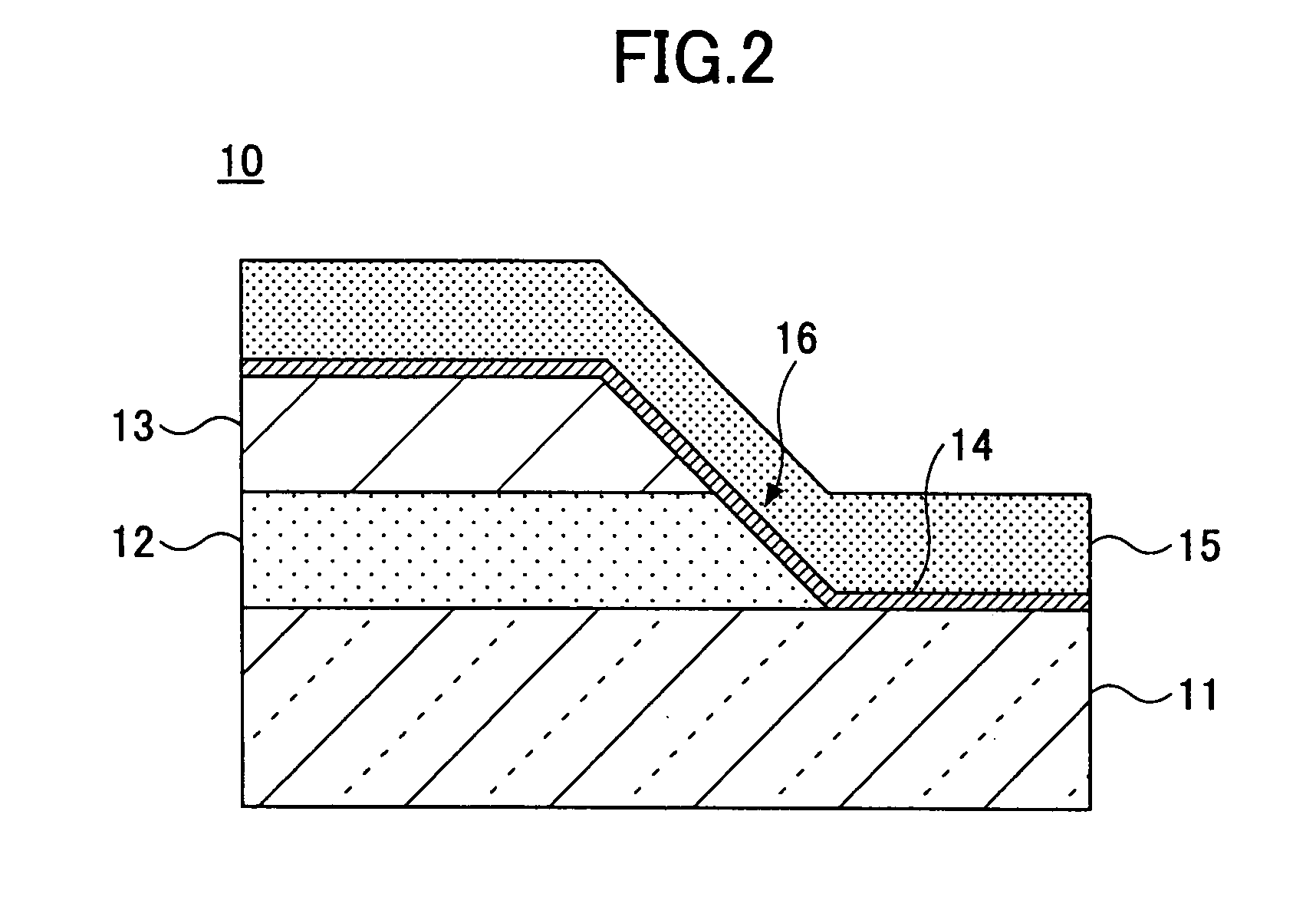
FIG. 2 is a cross sectional view showing a Josephson device in a first embodiment of the present invention.
A Josephson device 10 of the first embodiment shown in FIG. 2 has the ramp-edge structure. The Josephson device 10 has a substrate 11, a lower electrode layer 12 formed on the substrate 11, an insulator layer 13 covering the lower electrode layer 12, a barrier layer 14, and an upper electrode layer 15 covering the barrier layer 14. The barrier layer 14 covers a surface of the substrate 11, a sloping surface formed at one end of each of the lower electrode layer 12 and the insulator layer 13, and a surface of the insulator layer 13. A superconducting junction 16 is formed by the lower electrode layer 12, the barrier layer 14 and the upper electrode layer 15.
The substrate 11 is made of a material having a crystal structure that allows epitaxial growth of the lower electrode layer 12 on the substrate 11. For example, the substrate 11 may be made of a material selected from a group...
embodiment sample emb1-1
Embodiment samples Emb1-1 were formed to have the same structure as the Josephson device 10 shown in FIG. 2 including the barrier layer 14 formed by the ramp-edge type deposition layer.
First, a YBa2Cu3Oy layer was formed, as a lower electrode layer, on a MgO substrate to a thickness of 200 nm by magnetron sputtering using a YBa2Cu3Oy target, at a substrate temperature of 740° C., an Ar+10 Vol. % O2 atmosphere, and a pressure of 80 mTorr, where Vol. % denotes volume percent. Then, a SrSnO3 layer was formed, as an insulator layer, on the lower electrode layer to a thickness of 250 nm by magnetron sputtering using a SrSnO3 target, at a substrate temperature of 680° C., an Ar+50 Vol. % O2 atmosphere, and a pressure of 50 mTorr.
Thereafter, the lower electrode layer and the insulator were etched by Ar ions using as a mask a resist layer having an opening formed by photolithography in a region where a superconducting junction is to be formed, so as to form a sloping surface by the lower el...
emb1-1
When the embodiment samples Emb1-1 and the comparison samples Cmp1-1 are compared, it may be seen that the IcRn product of the embodiment samples Emb1-1 is larger than that of the comparison samples Cmp1-1 by 30% or more. It may be regarded that the improved IcRn product of the embodiment samples Emb1-1 is due to the increased Cu content (cation ratio) of the barrier layer, since the Cu content of the barrier layer of the embodiment samples Emb1-1 is 11 At. % larger than that of the comparison samples Cmp1-1.
FIG. 7 is a cross sectional view, on an enlarged scale, showing a superconducting junction for explaining a composition analysis method for use in a vicinity of the barrier layer.
The composition analysis of the superconducting junction that is formed by the lower electrode, the barrier layer and the upper electrode layer of the comparison samples Cmp1-1 was made by irradiating an electron beam having a beam diameter of 1 nm perpendicularly to the cross section of the superconduc...
PUM
| Property | Measurement | Unit |
|---|---|---|
| diameter | aaaaa | aaaaa |
| critical temperature | aaaaa | aaaaa |
| temperatures | aaaaa | aaaaa |
Abstract
Description
Claims
Application Information


