Flash storage chip and flash array storage system
- Summary
- Abstract
- Description
- Claims
- Application Information
AI Technical Summary
Benefits of technology
Problems solved by technology
Method used
Image

Examples
first embodiment
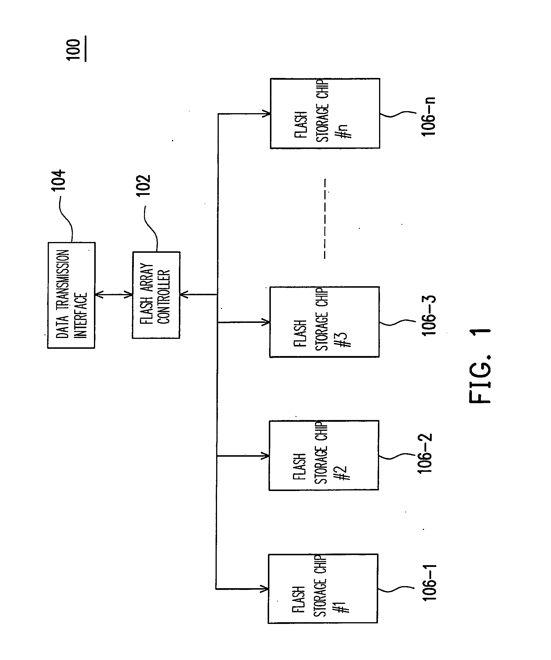
[0046]FIG. 1 is a block diagram of a flash array storage system according to the first embodiment of the present invention.
[0047] Referring to FIG. 1, the flash array storage system 100 includes a flash array controller 102, a data transmission interface 104, and a plurality of flash storage chips 106-1˜106-n.
[0048] The flash array controller 102 controls the distribution of data while writing data into the flash array storage system 100 and the searching of data while reading data from the flash array storage system 100. To be specific, the flash array controller 102 deems the flash storage chips 106-1˜106-n as logically continuous storage media and receives an instruction from a host (not shown) to access the flash storage chips 106-1˜106-n. When the host writes a data into the flash array storage system 100, the flash array controller 102 designates at least one of the flash storage chips 106-1˜106-n to write the data, and when the host reads a data from the flash array storage...
second embodiment
[0061]FIG. 3 is a block diagram of a flash array storage system according to the second embodiment of the present invention.
[0062] Referring to FIG. 3, the flash array storage system 300 includes a flash array driving program 302 and a plurality of flash storage chips 306-1˜306-n.
[0063] The flash array driving program 302 is executed by a host (not shown) for controlling the distribution of data while writing data into the flash array storage system 300 and the searching of data while reading data from the flash array storage system 300. To be specific, the flash array driving program 302 deems the flash storage chips 306-1˜306-n logically continuous storage media and receives an instruction from the host to access the flash storage chips 306-1˜306-n. When the host writes a data into the flash array storage system 300, the flash array driving program 302 designates at least one of the flash storage chips 306-1˜306-n to write the data, and when the host reads a data from the flash ...
PUM
 Abstract
Description
Claims
Application Information
PatSnap Eureka turns technology decisions into work you can execute. Powered by our Innovation Knowledge Graph, it runs expert workflows across engineering, life sciences, materials and intellectual property. Get your review-ready output in minutes.


