Data read-out circuit in semiconductor memory device and method of data reading in semiconductor memory device

a data read-out circuit and memory device technology, applied in the direction of error detection/correction, digital storage, instruments, etc., can solve the problems of data dissipation, microcomputer malfunction, data dissipation, etc., to improve the reliability of output data, reduce the malfunction of the device provided with the semiconductor memory device, and improve the reliability of the output data output.

Active Publication Date: 2008-02-28
RENESAS ELECTRONICS CORP
View PDF8 Cites 11 Cited by
  • Summary
  • Abstract
  • Description
  • Claims
  • Application Information

AI Technical Summary

Benefits of technology

[0011]As described above, the plurality kinds of read data are generated with regard to the same stored data. Even if a bit error exists in a read data obtained by using a certain reference level, the bit error may not appear in another read data obtained by using another reference level. Since the plurality kinds of read data are output from the sense amplifier circuit, the selector can select the most preferable one from the plurality kinds of read data. Therefore, reliability of the output data output from a semiconductor memory device provided with the read-out circuit is improved. Since the reliability of the output data is improved, malfunction of a device provided with the semiconductor memory device is reduced.
[0012]The above-mentioned control signal indicates, for example, respective numbers of error bits in the plurality of read data which are detected by an ECC (Error Correction Code) circuit. The selector can select a data corresponding to one of the plurality of read data having the minimum number of error bits, as the most preferable output data. For example, let us consider a case where one error bit exists in a read data obtained by using a certain reference level, while two error bits exist in another read data obtained by using another reference level. In this case, the read data including the one error bit is correctable by the ECC circuit. Therefore, the selector can output the post-correction-processing data as the most preferable output data. As a result, the malfunction of the device provided with the semiconductor memory device is prevented, and it is thus not necessary to stop the device.
[0015]According to the present invention, the reliability of the output data output from the data read-out circuit in the semiconductor memory device is improved. Since the reliability of the output data is improved, malfunction of a device provided with the semiconductor memory device is reduced.

Problems solved by technology

This leads to variation in the stored data (so-called “data dissipation” or “data corruption”).
The variation in the stored data causes malfunction of a microcomputer provided with the semiconductor memory device.
However, if there exist error bits more than the correctable number of bits in the read-out data, even the ECC circuit cannot correct the read-out data.
In this case, the malfunction of the microcomputer still occurs and thus the microcomputer fails.
If there exist error bits more than the correctable number of bits in the one kind of read data output from the sense amplifier circuit, the correction of the read data is no longer possible.

Method used


Image

  • Data read-out circuit in semiconductor memory device and method of data reading in semiconductor memory device
  • Data read-out circuit in semiconductor memory device and method of data reading in semiconductor memory device
  • Data read-out circuit in semiconductor memory device and method of data reading in semiconductor memory device

Examples


first embodiment

1. First Embodiment

1-1. Configuration and Operation

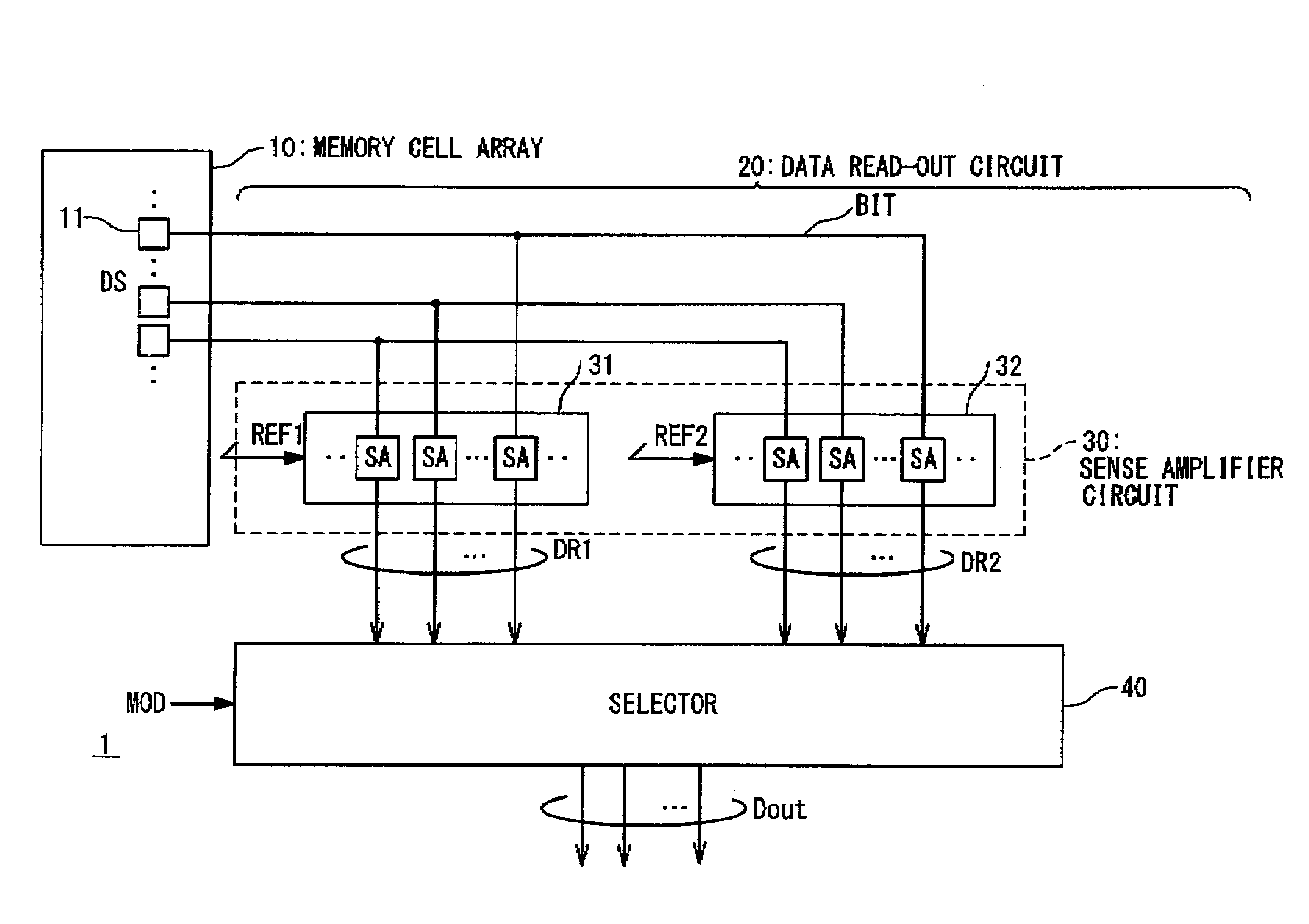
[0035]FIG. 1 schematically shows a configuration of a semiconductor memory device 1 according to the first embodiment. The semiconductor memory device 1 is provided with a memory cell array 10 and a data read-out circuit 20. The memory cell array 10 has a plurality of memory cells 11 arranged in an array form. Data stored in the memory cells 11 of the memory cell array 10 is hereinafter referred to as “stored data DS”.

[0036]The data read-out circuit 20 reads out the stored data DS from the memory cell array 10 and outputs the read data as an output data Dout. In the present embodiment, the data read-out circuit 20 includes: a sense amplifier circuit 30 connected to the memory cell array 10; and a selector 40 connected to the sense amplifier circuit 30.

[0037]The sense amplifier circuit 30 reads out the stored data DS from the memory cell array 10 and outputs the read data to the selector 40. More specifically, the sense amplifier cir...

second embodiment

2. Second Embodiment

[0079]FIG. 8 schematically shows a configuration of a semiconductor memory device 1 according to the second embodiment. In FIG. 8, the same reference numerals are given to the same components as those described in the first embodiment, and an overlapping description will be appropriately omitted.

[0080]In the foregoing first embodiment, the sense amplifier circuit 30 has the first sense amplifier circuit 31 and the second sense amplifier circuit 32, separately, and outputs the two kinds of read data DR1 and DR2 in parallel. In the second embodiment, the sense amplifier circuit 30 sequentially outputs the two kinds of read data DR1 and DR2. More specifically, the sense amplifier circuit 30 receives the first reference level REF1 and the second reference level REF2 in turn. The sense amplifier circuit 30 generates the first read data DR1 and the second read data DR2 in turn by using the first reference level REF1 and the second reference level REF2, respectively.

[00...

third embodiment

3. Third Embodiment

3-1. Configuration and Operation

[0084]FIG. 9 schematically shows a configuration of a semiconductor memory device 1 according to the third embodiment. In FIG. 9, the same reference numerals are given to the same components as those described in the first embodiment, and an overlapping description will be appropriately omitted.

[0085]According to the present embodiment, an ECC (Error Correction Code) circuit 60 is provided between the sense amplifier circuit 30 and the selector 40. The ECC circuit 60 executes an error correction processing with respect to the first read data DR1 and the second read data DR2. The performance of the error correction is determined based on required reliability and so forth. For example, the ECC circuit 60 is configured to be capable of detecting up to two bit errors and correcting up to one bit error. An error correction code ECC is used for the error correction processing.

[0086]As shown in FIG. 9, the memory cell array 10 includes a d...


PUM


Abstract

A data read-out circuit is provided with a sense amplifier circuit and a selector. The sense amplifier circuit senses a stored data stored in a memory cell array by using a plurality of reference levels to generate a plurality of read data, respectively. Thus, the sense amplifier circuit outputs the plurality of read data with regard to the stored data. The selector selects a data corresponding to any one of the plurality of read data based on a control signal and outputs the selected data as an output data.

Description

BACKGROUND OF THE INVENTION[0001]1. Field of the Invention[0002]The present invention relates to techniques of data reading in a semiconductor memory device.[0003]2. Description of Related Art[0004]Semiconductor memory devices such as a DRAM (Dynamic Random Access Memory), an EEPROM (Electrically Erasable and Programmable Read Only Memory), a flash memory and the like are known. In general, at the time of data reading in such a semiconductor memory device, a read-out level read out from a memory cell is compared with a predetermined reference level and thereby a data stored in the memory cell is judged (determined).[0005]Japanese Laid-Open Patent Application JP-P2005-209304A describes a technique in which data is judged by using a first reference potential and a second reference potential. According to the technique, the settings of the first reference potential and the second reference potential are designed to improve data-judgment precision in a sense amplifier circuit. The sense...

Claims


Application Information

Patent Timeline
Patent Type & Authority Applications(United States)
IPC IPC(8): G11C29/00G11C7/10
CPCG06F11/1004G11C7/04G11C7/1006G11C2029/0411G11C7/1051G11C7/106G11C7/1045
Inventor OKU, SATORU
Owner RENESAS ELECTRONICS CORP
Why Eureka
Try Eureka