Printed circuit board and method of manufacturing the same

a printed circuit board and manufacturing method technology, applied in printed circuit aspects, high frequency circuit adaptations, conductive pattern formation, etc., can solve the problems of difficult to form wiring having 50/b> or fewer pitches, difficult to realize wiring having 60 or fewer pitches, and difficult to use them as insulating materials, etc., to achieve high-functional, highly reliable fine circuits

Inactive Publication Date: 2008-03-06
SAMSUNG ELECTRO MECHANICS CO LTD
View PDF12 Cites 25 Cited by
  • Summary
  • Abstract
  • Description
  • Claims
  • Application Information

AI Technical Summary

Benefits of technology

[0009] Accordingly, in order to overcome the above problems occurring in the prior art, extensive research has been carried out. The result of this research is a thin printed circuit board, in which a pair of high-functional resin substrates having a permittivity ranging from 1.5 to 4.0, on one surface of each of which a circui...

Problems solved by technology

However, it is difficult to realize wiring having 60 or fewer pitches using a method of forming circuits on a Copper Clad Laminate (CCL), which is a base substrate, using a typical etching process (for example, a subtractive method).
Further, it is difficult to form wiring having 50 or fewer pitches using a method of reducing the thickness of the copper foil of a CC...

Method used


Image

  • Printed circuit board and method of manufacturing the same
  • Printed circuit board and method of manufacturing the same
  • Printed circuit board and method of manufacturing the same

Examples


Embodiment Construction

[0026] The present invention will be described in detail with reference to the accompanying drawings below.

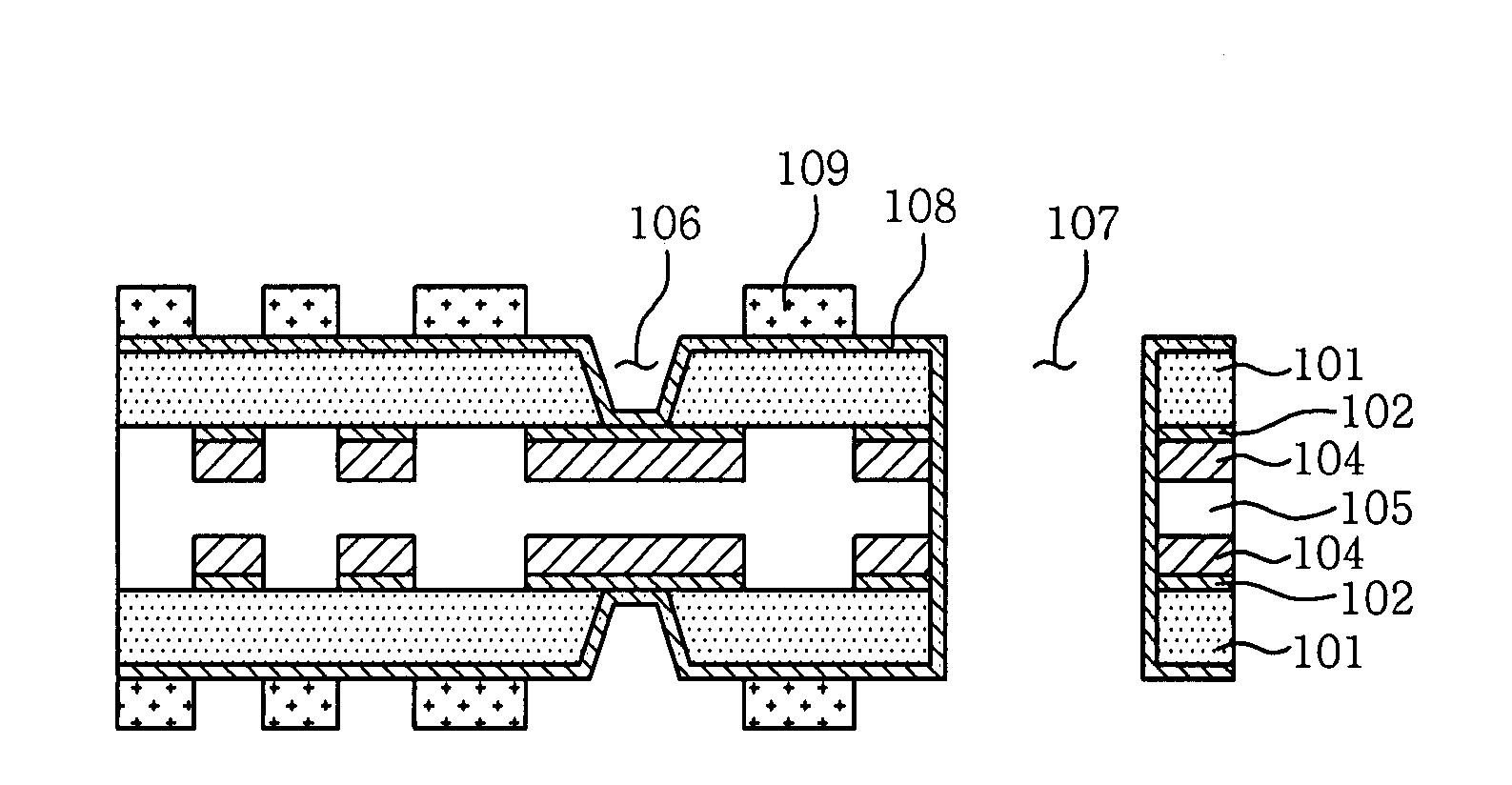
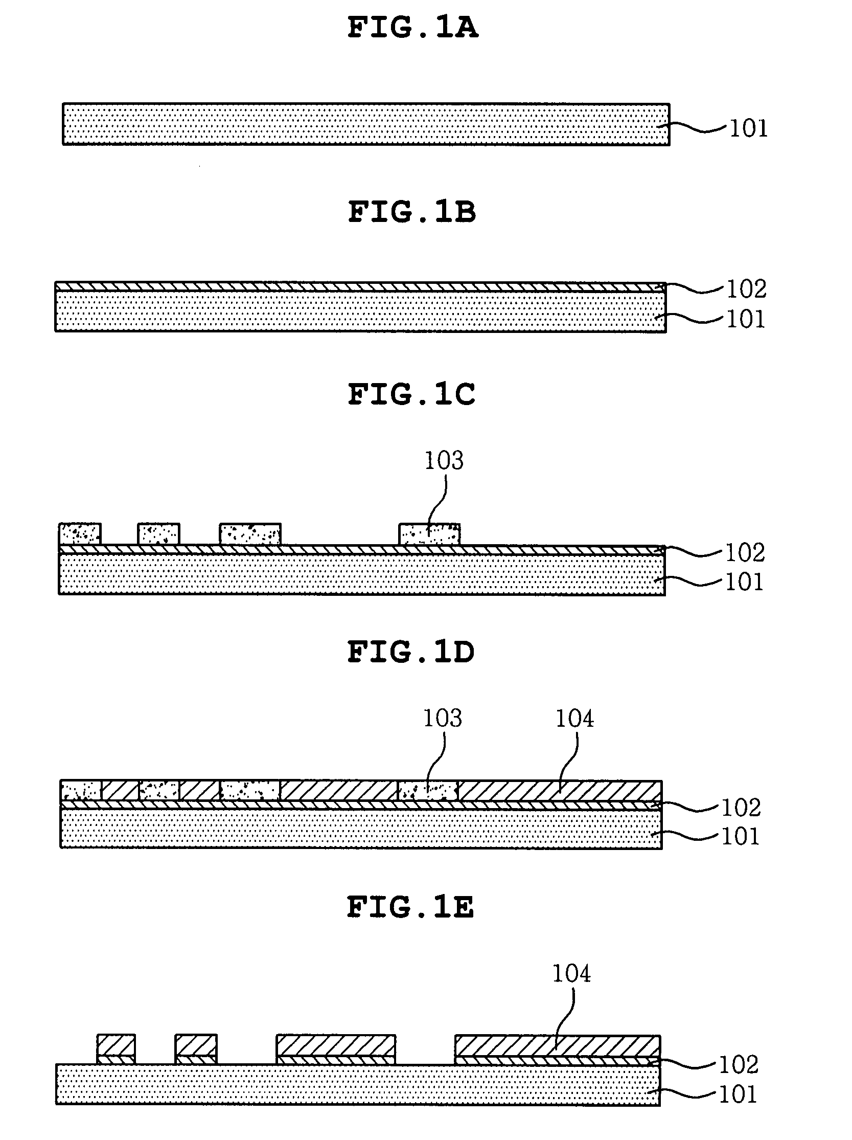
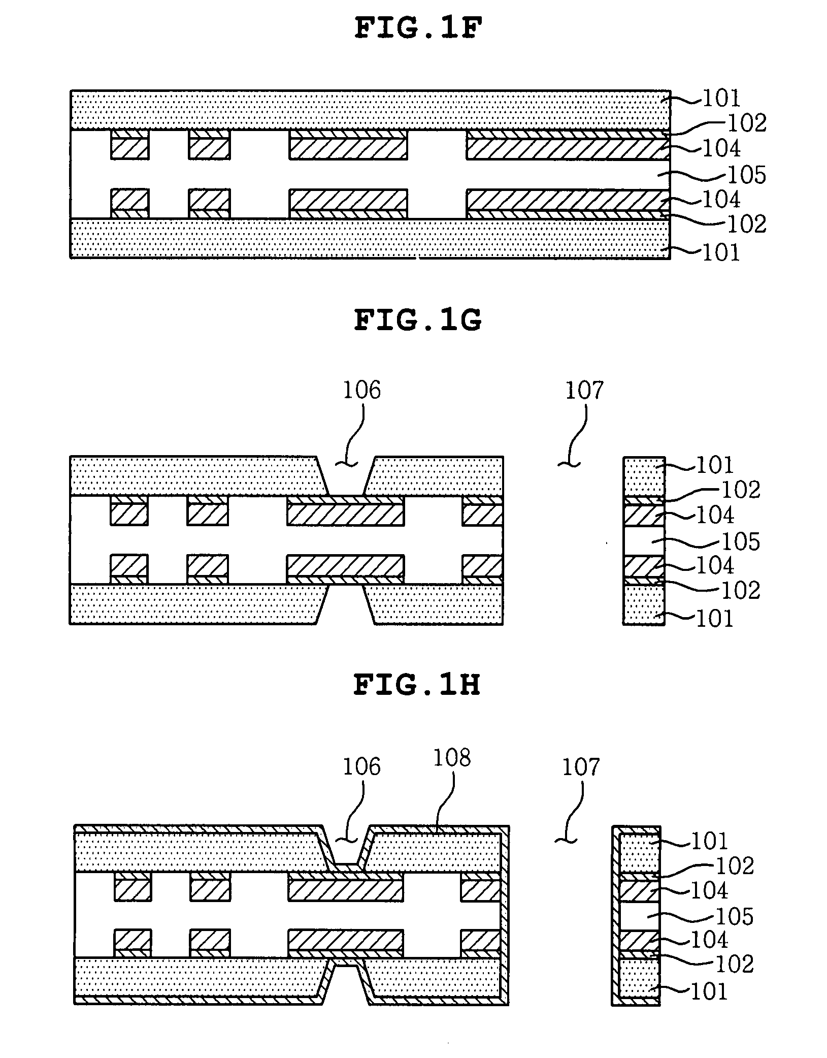
[0027] The present invention provides a high-functional thin printed circuit board and a method of manufacturing the printed circuit board, in which a pair of substrates, in each of which a copper layer is formed on a high-functional resin, such as PolyImide (PI), Liquid Crystal Polymer (LCP), or PolyTetraFluoroEthylene (PTFE), having a permittivity ranging from about 1.5 to about 4.0, through ion-beam surface treatment and vapor deposition, and a circuit pattern is formed in the copper layer, are layered with an insulating layer interposed therebetween, one or more through holes and one or more via holes are formed in the remaining surfaces of the respective layered substrates, and external circuit patterns are formed.

[0028]FIGS. 1A to 1J schematically show the flow of a process of manufacturing a printed circuit board according to a first embodiment of the present invention...


PUM

PropertyMeasurementUnit
Thicknessaaaaaaaaaa
Adhesivityaaaaaaaaaa
Permittivityaaaaaaaaaa

Abstract

Disclosed herein are a thin printed circuit board, in which a pair of high-functional resin substrates having a permittivity ranging from 1.5 to 4.0, on one surface of each of which a circuit pattern is formed through ion-beam surface treatment, vapor deposition and electroplating, are layered with an insulating layer interposed therebetween, and a method of manufacturing the printed circuit board. The circuit patterns are positioned inside the substrates. Thereafter, external layers are formed through ion-beam surface treatment, vapor deposition and electroplating. According to the present invention, the adhesiveness between each of the substrates and a metal layer may be improved through the ion-beam surface treatment/vapor deposition. Furthermore, since the pair of resin substrates are layered with the insulating layer interposed therebetween, the circuit patterns may be disposed inside the pair of resin substrates, so that the total thickness of the substrate may be reduced, thereby realizing highly reliable fine circuits.

Description

CROSS REFERENCE TO RELATED APPLICATIONS [0001] This application claims the benefit of Korean Patent Application No. 10-2006-0084184, filed on Sep. 1, 2006, entitled “Printed Circuit Board and Manufacturing Method Thereof,” and Korean Patent Application No. 10-2007-0074625, filed on Jul. 25, 2007, entitled “Printed Circuit Board and Manufacturing Method Thereof,” which are hereby incorporated by reference in their entirety in this application. BACKGROUND OF THE INVENTION [0002] 1. Field of the Invention [0003] The present invention relates generally to a printed circuit board and a method of manufacturing the printed circuit board. More particularly, the present invention relates to a printed circuit board and a method of manufacturing the printed circuit board, in which a pair of high-functional resin substrates, on one surface of each of which a circuit pattern is formed through ion-beam surface treatment, vapor deposition and electroplating, are layered with an insulating layer in...

Claims


Application Information

Patent Timeline
IPC IPC(8): H05K1/00H05K3/10
CPCH05K1/024Y10T29/49155H05K3/205H05K3/381H05K3/388H05K3/4069H05K3/4602H05K3/4614H05K3/4632H05K3/4644H05K3/4647H05K2201/0141H05K2201/015H05K2201/0154H05K2201/0376H05K2203/092H05K3/108
Inventor PARK, JUN HEYOUNGKIM, TAEHOONKIM, DONG SUNHER, SAM JINKIM, SEUNG CHUL
Owner SAMSUNG ELECTRO MECHANICS CO LTD
Why Eureka
Try Eureka