Semiconductor device package, semiconductor apparatus, and methods for manufacturing the same
Active Publication Date: 2008-03-06
SHINKO ELECTRIC IND CO LTD
View PDF7 Cites 30 Cited by
Summary
Abstract
Description
Claims
Application Information
AI Technical Summary
This helps you quickly interpret patents by identifying the three key elements:
Problems solved by technology
Method used
Benefits of technology
Benefits of technology
[0013]More specifically, the present invention is directed to increase the reliability of a package formed by using a silicon substrate, and mounting of a semiconductor apparatus including a semiconductor device mounted on the package.
[0026]As a whole to say, this invention can improve the reliability of mounting of a semiconductor apparatus with a semiconductor device being mounted on a silicon substrate.
Problems solved by technology
However, when a via hole penetrating through a silicon substrate is formed, the defective shape (variation in shape) of the via hole may occur.
In general, such a defective shape is more likely to occur in the opening portion of the via hole.
For example, performing the dry etching with using a mask pattern, problems of fine peeling, defective shape, or the like tend to occur at the interface between the silicon substrate and the mask pattern.
For this reason, various defective shapes of etching occur due to the problem of the mask pattern in the vicinity of the opening.
This entails the fear that the damage (such as chipping or cracking) of the silicon substrate occurs.
Further, the occurrence of the defective shape of the via hole unfavorably deteriorates the reliability of the via plug.
Method used
Image
Click on the blue label to locate the original text in one second.
Reading with bidirectional positioning of images and text.
Examples
example 1
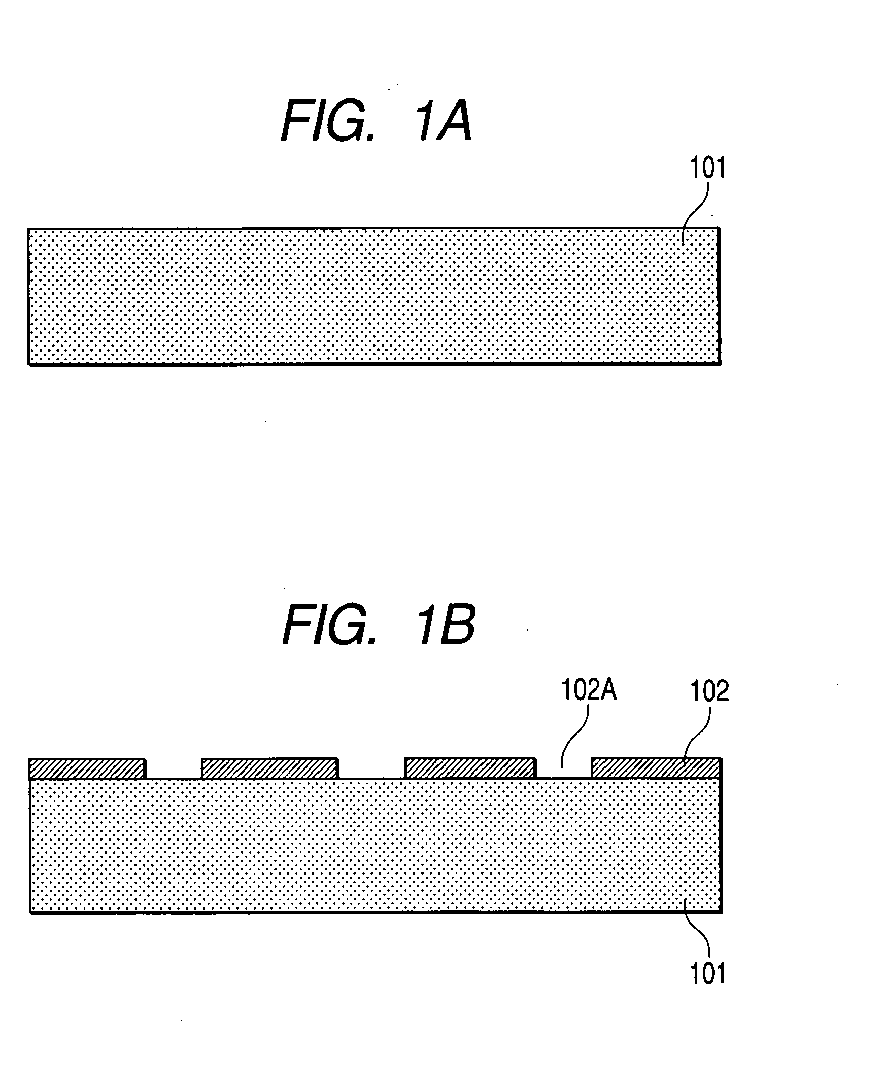
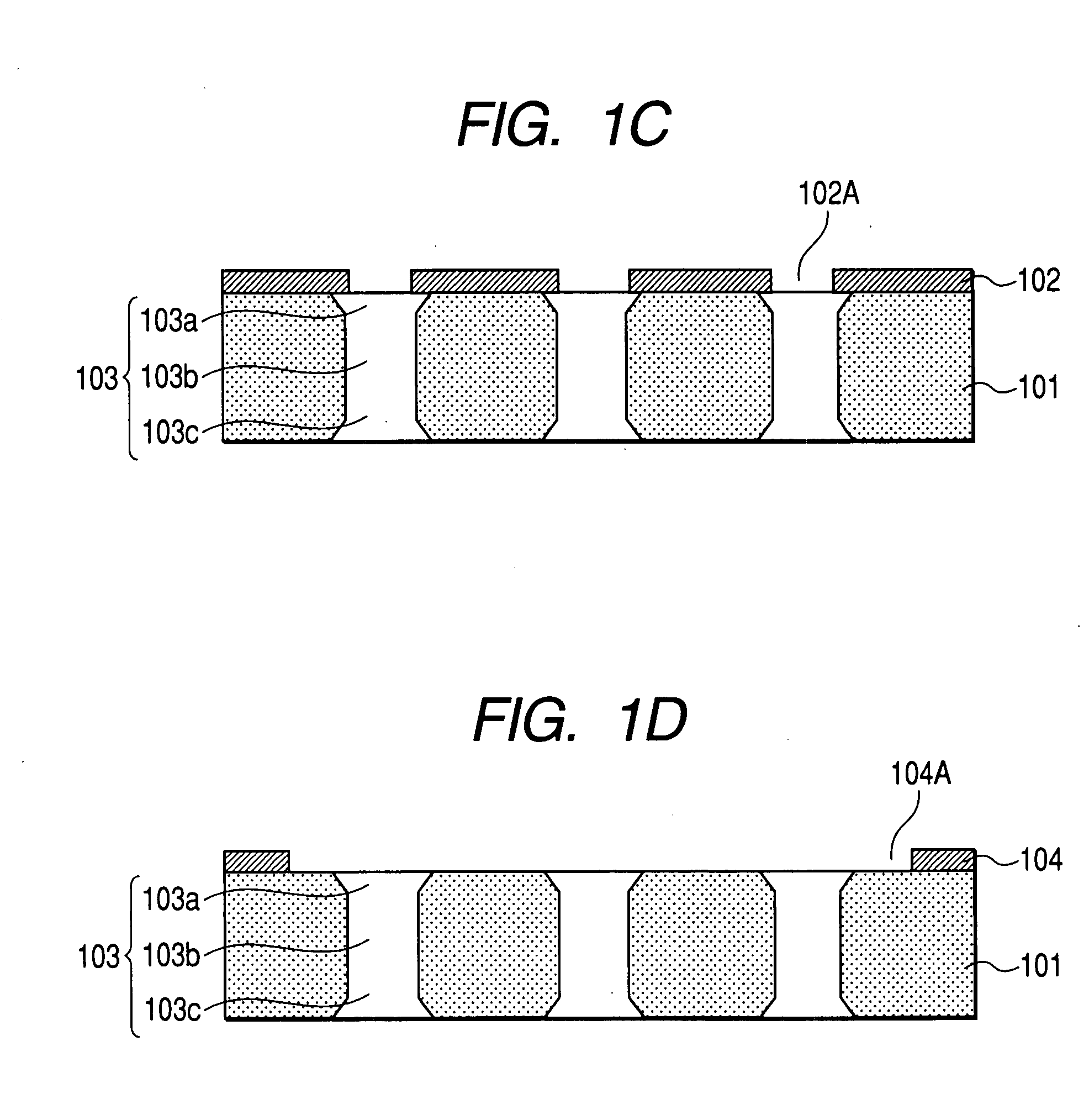
[0051]FIGS. 1A to 1G are views showing a method for manufacturing a package and a semiconductor apparatus step by step in accordance with Example 1 of the invention. Further, FIG. 1F shows the package to be manufactured, and further, FIG. 1G also shows the structure of the semiconductor apparatus to be manufactured using the package. However, in the following drawings, the devices described previously are given the same reference numerals and signs, and the description may be omitted.
[0052]First, in a step shown in FIG. 1A, a substrate made of silicon (e.g., a silicon wafer) 101 is prepared. For example, when the substrate 101 is formed of a silicon wafer, the thickness of the substrate 101 is in a range about from 600 to 800 μm. Alternatively, the substrate maybe ground such that the substrate 101 has a prescribed thickness.
[0053]Then, in a step shown in FIG. 1B, on the substrate 101, a mask pattern 102 having an opening 102A is formed. For forming the mask pattern 102, a resist la...
example 2
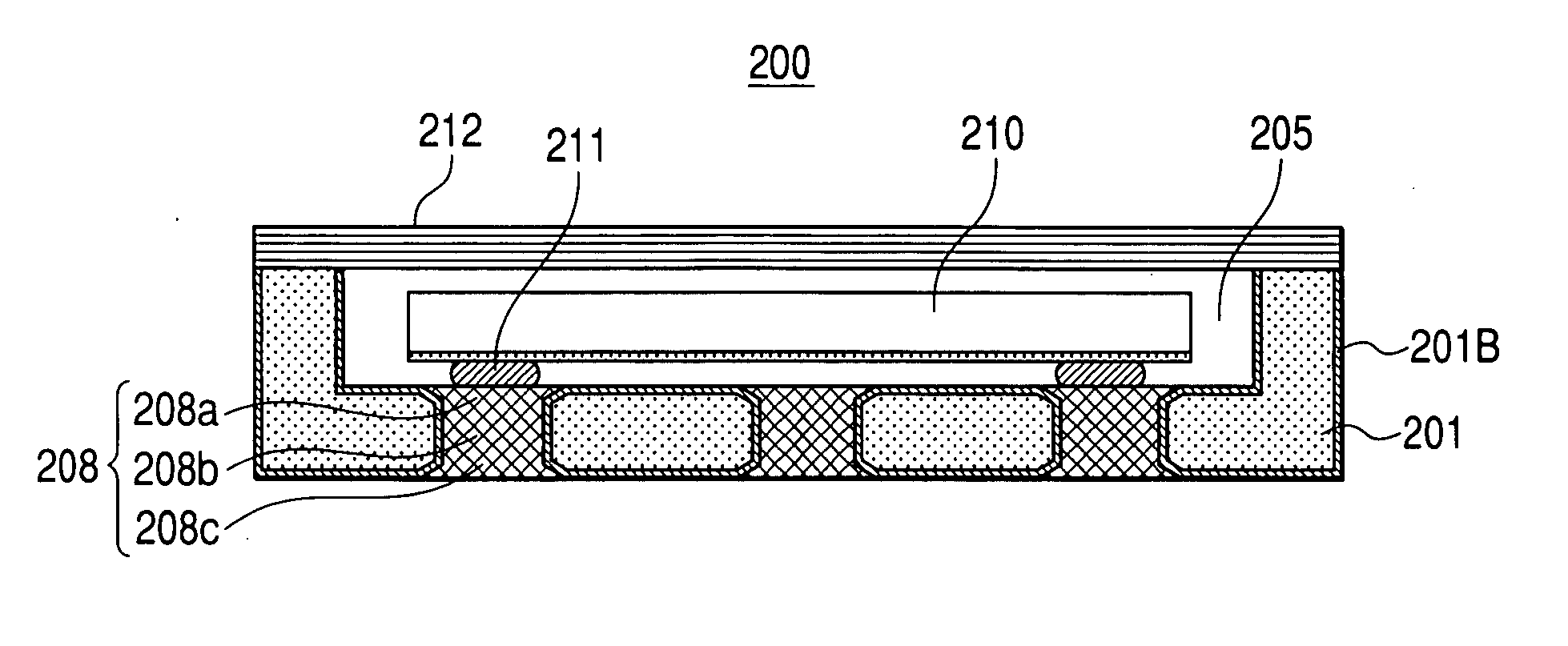
[0073]FIGS. 2A to 2K are views showing a method for manufacturing a package and a semiconductor apparatus step by step in accordance with Example 2 of the invention. Further, FIG. 2J shows the package to be manufactured, and further, FIG. 2K also shows the structure of the semiconductor apparatus to be manufactured using the package. However, in the following drawings, the devices described previously are given the same reference numerals and signs, and the description may be omitted.
[0074]First, a step shown in FIG. 2A corresponds to the step shown in FIG. 1A. A substrate 201 made of silicon corresponding to the silicon wafer 101 is prepared.
[0075]Then, in a step shown in FIG. 2B, in the same manner as the step shown in FIG. 1B, on the substrate 201, a mask pattern 202 having an opening 202A is formed. The opening 202A is formed at the position corresponding to a via hole (via plug) to be formed in a later step.
[0076]Then, in a step shown in FIG. 2C, a via hole (through hole) 203 p...
PUM
Abstract
A method for manufacturing a package which includes: an etching step of etching a silicon substrate, and forming a via hole penetrating through the silicon substrate; and a step of embedding an electrically conductive material in the via hole, and forming a via plug, characterized in that the etching step includes a first etching step of forming the via hole in a straight shape, and a second etching step of forming the via hole in a taper shape.
Description
[0001]This application claims foreign priority based on Japanese Patent application No. 2006-242021, filed on Sep. 6, 2006, the contents of which is incorporated herein by reference in its entirety.BACKGROUND OF THE INVENTION[0002]1. Field of the Invention[0003]The present invention relates to a semiconductor apparatus including a semiconductor device mounted on a silicon substrate, and a method for manufacturing the semiconductor apparatus.[0004]2. Description of the Related Art[0005]As for the structure of the semiconductor apparatus including a semiconductor device mounted on a substrate, various types of them have been proposed such as disclosed in Japanese unexamined patents 2005-19609 or 2005-327820.[0006]For example, when a silicon substrate is used for mounting a semiconductor device, micromachining on the substrate becomes possible. This enables a manufacturer to downsize a semiconductor apparatus. Further, silicon has higher thermal conductivity as compared with that of a ...
Claims
Application Information
Patent Timeline
Application Date:The date an application was filed.
Publication Date:The date a patent or application was officially published.
First Publication Date:The earliest publication date of a patent with the same application number.
Issue Date:Publication date of the patent grant document.
PCT Entry Date:The Entry date of PCT National Phase.
Estimated Expiry Date:The statutory expiry date of a patent right according to the Patent Law, and it is the longest term of protection that the patent right can achieve without the termination of the patent right due to other reasons(Term extension factor has been taken into account ).
Invalid Date:Actual expiry date is based on effective date or publication date of legal transaction data of invalid patent.

