Power gating circuit, system on chip circuit including the same and power gating method
- Summary
- Abstract
- Description
- Claims
- Application Information
AI Technical Summary
Benefits of technology
Problems solved by technology
Method used
Image

Examples
Embodiment Construction
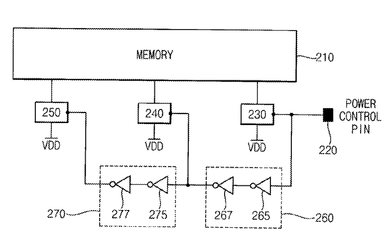
[0038]FIG. 2 is a block diagram illustrating a power gating circuit for a memory device 210 including an inverter delay chain 260 and 270.
[0039]Referring to FIG. 2, the power gating circuit includes a power control pin 220, power gating transistors 230, 240 and 250, a first inverter delay chain 260, and a second inverter delay chain 270. The first inverter delay chain 260 includes inverters 265 and 267. The second inverter delay chain 270 includes inverters 275 and 277.
[0040]When the first power gating transistor 230 is turned ON by a power control signal that is applied to the power control pin 220, a power supply voltage VDD is applied to a first pin of the memory device 210. When the second power gating transistor 240 is turned ON by the power control signal that is delayed through the first inverter chain 260, the power supply voltage VDD is applied to the first and second pin of the memory device 210. When the third power gating transistor 250 is turned ON by the power control ...
PUM
 Abstract
Description
Claims
Application Information
 - R&D Engineer
- R&D Manager
- IP Professional
- Industry Leading Data Capabilities
- Powerful AI technology
- Patent DNA Extraction
Browse by: Latest US Patents, China's latest patents, Technical Efficacy Thesaurus, Application Domain, Technology Topic.
© 2024 PatSnap. All rights reserved.Legal|Privacy policy|Modern Slavery Act Transparency Statement|Sitemap