Optical transmitter and drive method of same

Inactive Publication Date: 2008-03-06
FUJITSU LTD
View PDF5 Cites 33 Cited by
  • Summary
  • Abstract
  • Description
  • Claims
  • Application Information

AI Technical Summary

Benefits of technology

[0031]Accordingly, in consideration of the above-described problems, an object of the present invention is to provide an optical transmitter able to always optimally maintain the phase difference between the data signal and the clock signal (i) without employing a feed fo

Problems solved by technology

The above-described function units involve complex data processing, therefore processing is difficult at a high 40 Gb/s bit rate.
The problem 1 is that it is difficult to constantly keep the phase difference between the 40 Gb/s data signal D and the 20 GHz clock signal CK in FIG. 15 despite temperature fluctuations etc.
This invites deterioration of the transmission characteristic.
To hold this, it can be considered to employ for example feedback control, but in practice, there is the problem that it is actually difficult to acc

Method used


Image

  • Optical transmitter and drive method of same
  • Optical transmitter and drive method of same
  • Optical transmitter and drive method of same

Examples


first embodiment

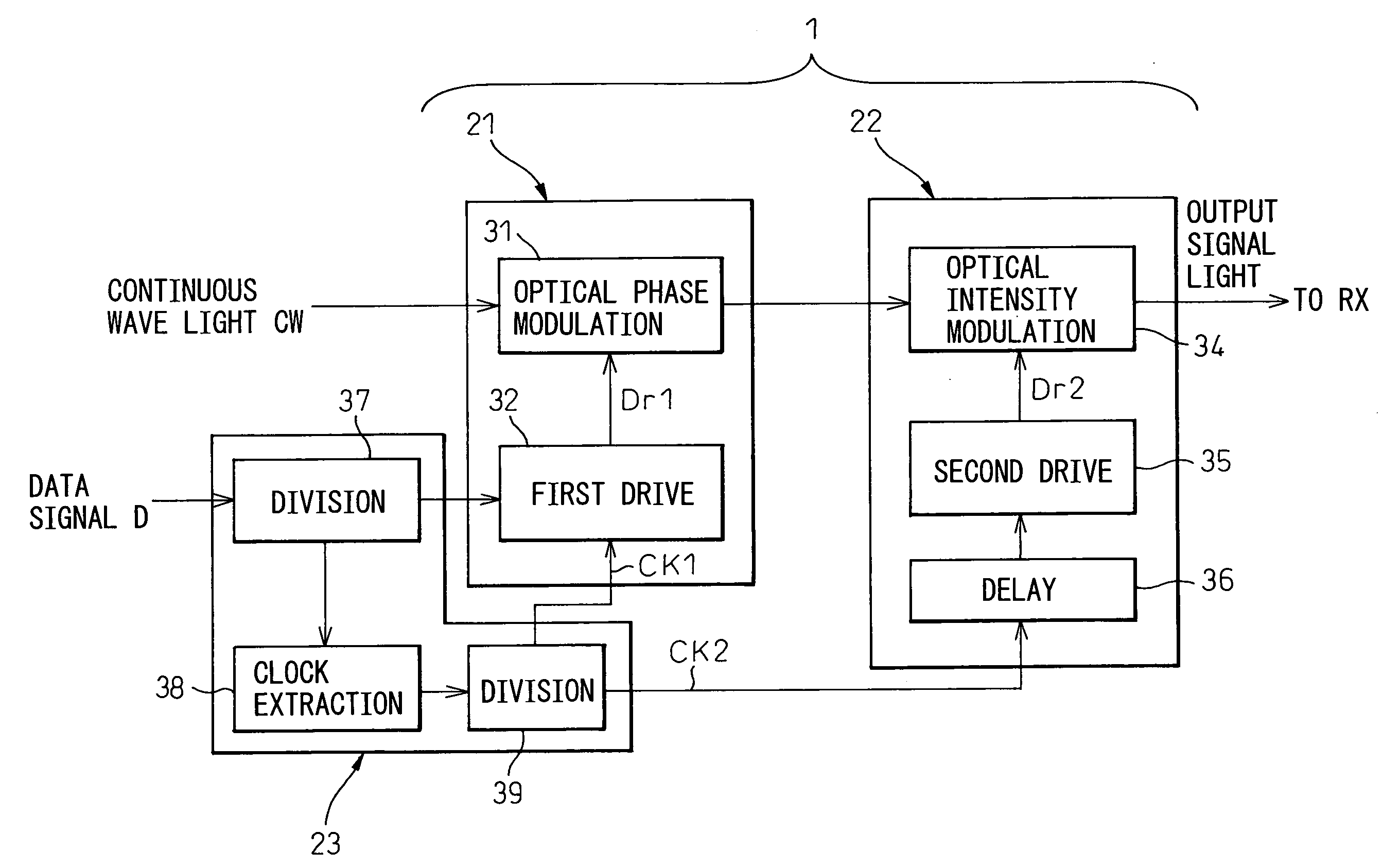
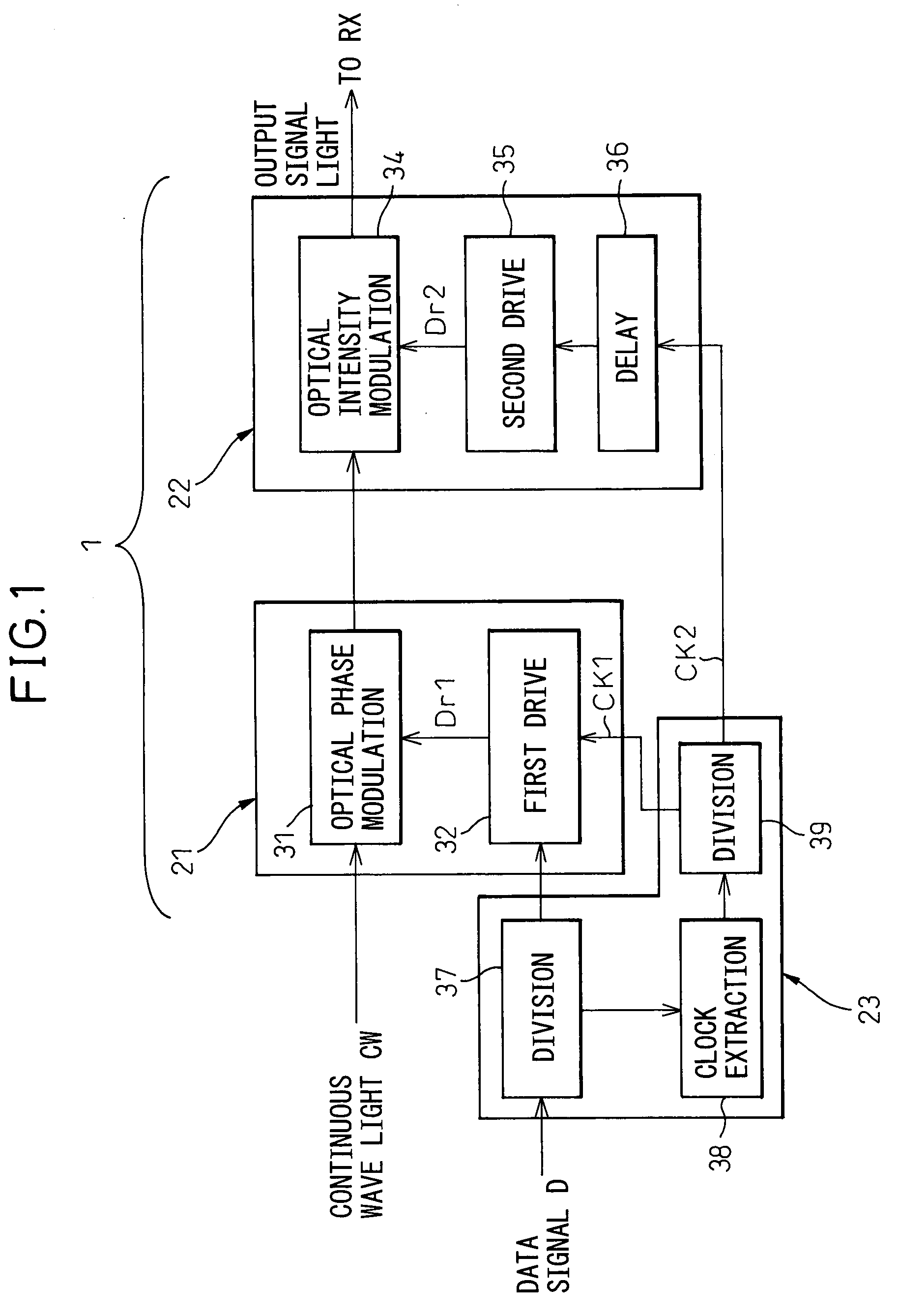
[0070]Next, several embodiments of the optical transmitter 1 driven according to the above-described drive method will be explained. FIG. 3 is a diagram showing an optical transmitter 1 according to the present invention. Note that the same reference numerals or symbols will be attached to the same components throughout all of the drawings.

[0071]Most of the configuration of FIG. 3 is the same as the conventional configuration shown in FIG. 15. The components newly introduced in the first embodiment are a first divider 41 (corresponding to 37 of FIG. 1), a PLL (phase locked loop) portion 42 (corresponding to 38 of FIG. 1), and a second divider 43 (corresponding to 39 of FIG. 1). This second divider 43 is equivalent to the divider 13 of FIG. 15. These components configure the clock recovery function unit 23 of FIG. 1. Further, on the optical intensity modulation function unit 22 side, a delay unit 45 (corresponding to 36 of FIG. 1) is introduced. Note that reference numeral 47 is a fi...

fourth embodiment

[0086]In short, in the fourth embodiment in which the intensity modulation is carried out by the CSRZ modulation scheme, the intensity modulation function unit 22 is configured by a frequency division unit 62 for performing ½ frequency division of the second clock signal CK2 comprised of the clock component having the same rate as that of the data signal D from the PLL portion 42′, a delay unit 45 for giving a constant delay to the ½ frequency divided signal thereof, and a second amplification unit 48 for amplifying the delay signal and outputting the second drive signal Dr2. That delay is set equal to the transmission delay when the data signal D passes through the FF portion 52 and the amplifier 14. Further, the second amplification unit 48 outputs a voltage two times the extinction voltage of the intensity modulation.

third embodiment

[0087]For this reason, in FIG. 6, in order to generate the above-described “½ frequency”, the aforesaid frequency division unit (½ frequency division) 62 is introduced, and the second clock signal CK2 of 20 GHz is ½ multiplied to 10 GHz. Note that, an explanation will be given of the extinction voltage with reference to FIG. 12.

[0088]In short, in the third embodiment in which the intensity modulation is carried out using the CSRZ modulation scheme, the intensity modulation function unit 22 is configured by a frequency division unit 62 for performing ½ frequency division of the second clock signal CK2 comprised of the clock component having a rate of ½ of that of the data signal D from the PLL portion 42, a delay unit 45 for giving a constant delay to the ½ frequency divided signal thereof, and a second amplification unit 48 for amplifying the delay signal and outputting the second drive signal Dr2. That delay is set equal to the transmission delay when the data signal D passes throu...


PUM


Abstract

An optical transmitter for performing optical phase modulation according to a data signal and further applying optical intensity modulation in synchronization with clock signals and transmitting the optical signals, wherein in order to maintain the phase difference between the data signal and the clock signal constant with a simple configuration, the optical transmitter is configured so that clock signals are not individually supplied from the outside, but a clock component thereof is extracted from the data signal itself and a clock signal recovered based on the extracted clock component is defined as the clock signal. For this purpose, the configuration is made so that a clock recovery function unit is newly introduced.

Description

BACKGROUND OF THE INVENTION[0001]1. Field of the Invention[0002]The present invention relates to an optical transmitter, more particularly relates to an optical transmitter for applying phase modulation and intensity modulation to an optical signal and transmitting the result to a receiver, and a method of driving the optical transmitter.[0003]2. Description of the Related Art[0004]In recent years, demand has been rising for introduction of the next generation 40 Gbit / s (Gb / s) optical transmission system. In addition, a transmission distance and efficiency of frequency utilization equivalent to those of the conventional 10 Gb / s optical transmission system are being demanded. As means able to meet these demands, there has been active R&D into the RZ-DPSK (return to zero-differential phase shift keying) modulation scheme or CSRZ-DPSK (carrier suppressed-DPSK) modulation scheme better in optical signal-to-noise ratio (OSNR) tolerance and non-linear tolerance in comparison with the NRZ ...

Claims


Application Information

Patent Timeline
IPC IPC(8): H04B10/12H04B10/04H04B10/40H04B10/07H04B10/2507H04B10/50H04B10/516H04B10/524H04B10/54H04B10/556H04B10/588H04B10/60H04B10/61
CPCH04B10/505H04B10/5051H04B10/5561H04B10/5165H04B10/5162
Inventor NISHIHARA, MASATOTAKAHARA, TOMOO
Owner FUJITSU LTD
Why Eureka
Try Eureka