Coating treatment method, computer-readable storage medium, and coating treatment apparatus

a technology of coating treatment and computer-readable storage medium, applied in the direction of coatings, photomechanical devices, instruments, etc., can solve the problems of inability to adjust the above-described parameters, inability to sufficiently uniformize the resist film, etc., and achieve the effect of improving the yield of the final substrate produ

Active Publication Date: 2008-03-06
TOKYO ELECTRON LTD
View PDF5 Cites 57 Cited by
  • Summary
  • Abstract
  • Description
  • Claims
  • Application Information

AI Technical Summary

Benefits of technology

[0009]According to the present invention, the solvent can be supplied to the thick portion of the coating solution at the third step to increase the flowability of the coating solution at the thick portion to thereby reduce the thickness of the coating solution of that portion. On the other hand, the dry gas can be supplied to the thin portion of the coating solution to decrease the flowability of the thin portion to thereby increase the thickness of the coating solution at that portion. As a result, a uniform coating film can be finally formed within the substrate.
[0012]According to the present invention, since a uniform coating film can be formed on a substrate, the yields of final substrate products can be improved.

Problems solved by technology

However, the adjustment of the above-described parameters cannot cope with local variations of the resist film within the wafer, failing to sufficiently uniform the resist film.

Method used


Image

  • Coating treatment method, computer-readable storage medium, and coating treatment apparatus
  • Coating treatment method, computer-readable storage medium, and coating treatment apparatus
  • Coating treatment method, computer-readable storage medium, and coating treatment apparatus

Examples


Embodiment Construction

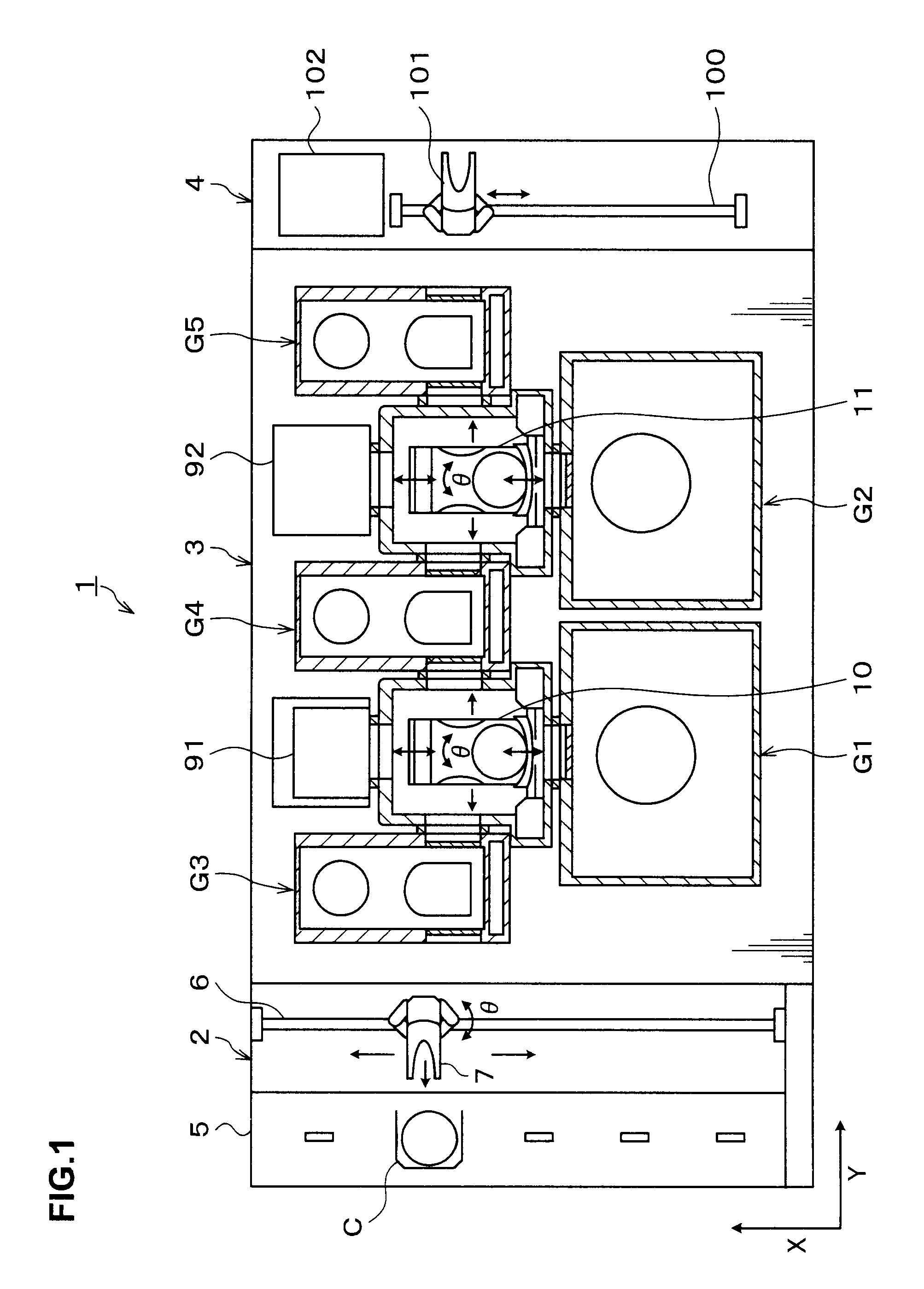
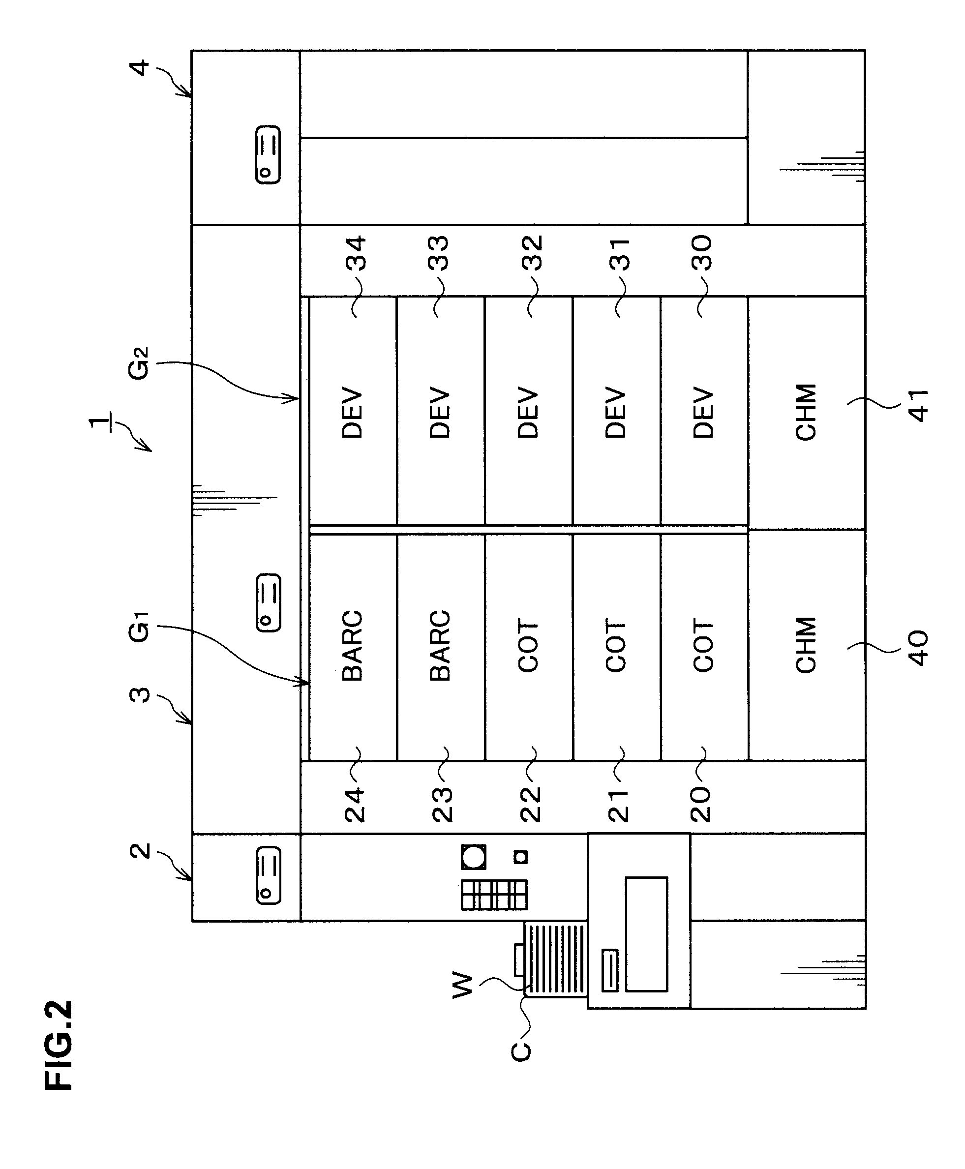
[0029]Hereinafter, a preferred embodiment of the present invention will be described. FIG. 1 is a plan view showing the outline of a configuration of a coating and developing treatment system 1 incorporating a coating treatment apparatus according to the embodiment, FIG. 2 is a front view of the coating and developing treatment system 1, and FIG. 3 is a rear view of the coating and developing treatment system 1.

[0030]The coating and developing treatment system 1 has, as shown in FIG. 1, a configuration in which, for example, a cassette station 2 for transferring a plurality of wafers W per cassette as a unit from / to the outside into / from the coating and developing treatment system 1 and transferring the wafers W into / out of a cassette C; a processing station 3 including a plurality of various kinds of processing and treatment units, which are multi-tiered, for performing predetermined processing or treatment in a manner of single wafer processing in the photolithography process; and...


PUM


Abstract

In the present invention, a substrate is first rotated at a first rotation speed, and a resist solution is applied to the rotated substrate. Subsequently, the rotation of the substrate is decelerated to a second rotation speed lower than the first rotation speed so that the substrate is rotated at the low speed to smooth the resist solution on the substrate. The rotation of the substrate is then accelerated to a third rotation speed higher than the second rotation speed, and a solvent for the coating solution and / or a dry gas are / is supplied to the resist solution on the substrate. In this event, the solvent gas is supplied to a portion of the resist solution on the substrate thicker than a set thickness, and the dry gas is supplied to a portion of the coating solution on the substrate thinner than the set thickness. This thins the thicker portion of the resist solution and thickens the thinner portion to uniform the resist solution.

Description

BACKGROUND OF THE INVENTION[0001]1. Field of the Invention[0002]The present invention relates to a coating treatment method, a computer-readable storage medium storing a program, and a coating treatment apparatus.[0003]2. Description of the Related Art[0004]In a photolithography process in manufacturing, for example, a semiconductor device, for example, a resist coating treatment for applying a resist solution onto a wafer to form a resist film, exposure processing for exposing the resist film into a predetermined pattern, and developing treatment for developing the exposed resist film are performed in sequence to form a predetermined resist pattern on the wafer.[0005]In the above-described resist coating treatment, the wafer is rotated at a high speed, and a predetermined amount of the resist solution is supplied to the central portion of the rotated wafer and spread to the entire surface of the wafer by the centrifugal force. Subsequently, the rotation of the wafer is decelerated ...

Claims


Application Information

Patent Timeline
Patent Type & Authority Applications(United States)
IPC IPC(8): B05D1/40B05C9/08
CPCH01L21/6715G03F7/162
Inventor TANAKA, TAKASHI
Owner TOKYO ELECTRON LTD
Why Eureka
Try Eureka