Adhesive sheet for water jet laser dicing

Inactive Publication Date: 2008-03-06
NITTO DENKO CORP
View PDF5 Cites 4 Cited by
  • Summary
  • Abstract
  • Description
  • Claims
  • Application Information

AI Technical Summary

Benefits of technology

[0009]It is an object of the present invention to provide an adhesive sheet with which adequate expandability can be obtained in pick-up after dicing, while maintaining the transmissivity of the liquid used in

Problems solved by technology

However, physical stress produced by the dicing blade can cause die fly-off in the chips and the like cut by this method, or cause cracking, chipping, and other such defects, which lowers the quality of the chips and the like, and also lowers the efficiency of this cutting method.
This problem has become more serious as there has been greater demand for even smaller and thinner electronic devices in recent years.
Also, with a cutting method that makes use of this laser technique, the use of a water jet can be a problem in that it makes the chips or the like more susceptible to coming loose from the

Method used


Image

  • Adhesive sheet for water jet laser dicing
  • Adhesive sheet for water jet laser dicing

Examples


example 1

[0047]An acrylic adhesive composed of 100 parts acrylic copolymer, 30 parts plasticizer, and 10 parts crosslinking agent was used to coat one side of a 50 μm process liner in a thickness 15 μm, after which the coating was dried for 3 minutes at 100° C. After drying, the coating side was immediately applied to a base film (a blended film of EVA (vinyl content of 9%) and polyethylene (blend ratio (wt %) of EVA:polyethylene=30:70)) to obtain an adhesive sheet.

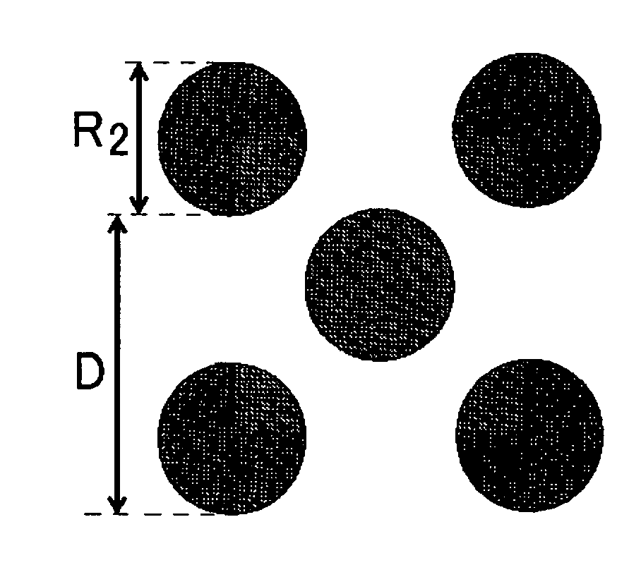
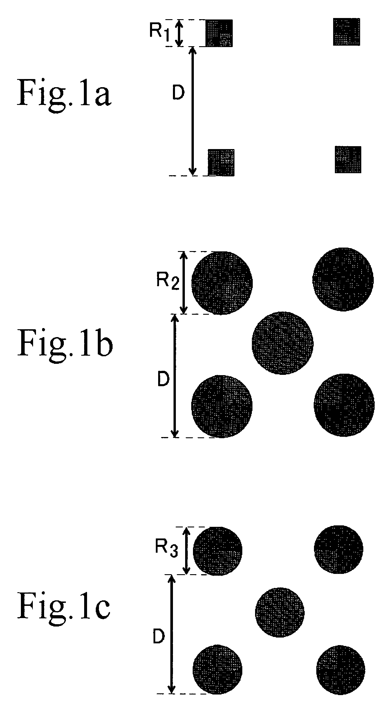
[0048]Perforations were made in the film thus produced by thermal machining using a laser with a wavelength of 1064 nm and a laser boring apparatus M4350 (made by esi), which gave an adhesive sheet for semiconductor wafer processing. Circular perforations with an area of 0.2 mm2 were made so that the spacing D of the perforations in FIG. 1b was 1 mm.

example 2

[0049]An acrylic adhesive composed of 100 parts acrylic copolymer, 30 parts plasticizer, and 10 parts crosslinking agent was used to coat one side of a 50 μm process liner in a thickness 15 μm, after which the coating was dried for 3 minutes at 100° C. After drying, the coating side was immediately applied to a base film (a blended film of EVA (vinyl content of 9%) and polyethylene (blend ratio (wt %) of EVA:polyethylene=30:70)) to obtain an adhesive sheet.

[0050]The above-mentioned film was machined with a precision film punching machine (RFP-S20, made by UHT), which gave an adhesive sheet for semiconductor wafer processing in which circular perforations with an area of 0.2 mm2 were made so that the spacing D of the perforations in FIG. 1b was 1 mm.

example 3

[0051]An acrylic adhesive composed of 100 parts acrylic copolymer, 30 parts plasticizer, and 10 parts crosslinking agent was used to coat one side of a 50 μm process liner in a thickness 15 μm, after which the coating was dried for 3 minutes at 100° C. After drying, the coating side was immediately applied to a base film (a blended film of EVA (vinyl content of 9%) and polyethylene (blend ratio (wt %) of EVA:polyethylene=30:70)) to obtain an adhesive sheet.

[0052]A rotary roll equipped on its surface with hollow needles for making perforations was used, which gave an adhesive sheet for semiconductor wafer processing in which circular perforations with an area of 0.2 mm2 were made so that the spacing D of the perforations in FIG. 1b was 1 mm.


PUM

PropertyMeasurementUnit
Diameteraaaaaaaaaa
Areaaaaaaaaaaa
Elongationaaaaaaaaaa

Abstract

An adhesive sheet for water jet laser dicing, comprises an adhesive layer laminated on a base film, wherein the adhesive sheet has perforations, has a porosity of 3 to 90% and has a fracture elongation of at least 100%.

Description

BACKGROUND OF THE INVENTION[0001]1. Field of the Invention[0002]The present invention relates to an adhesive sheet for water jet laser dicing, and more particularly relates to an adhesive sheet for water jet laser dicing used to fix a semiconductor wafer and / or a semiconductor-related material during dicing with a water jet laser.[0003]2. Background Information[0004]The conventional practice has been to use a rotary blade known as a dicing blade to cut semiconductor wafers, semiconductor-related materials and the like, and separate them into chips and IC parts. In this dicing step, the semiconductor wafer or the like is usually affixed with an adhesive tape to fix it in place. After the semiconductor wafer or the like has been cut into chips, they are removed from the adhesive tape by a pick-up.[0005]However, physical stress produced by the dicing blade can cause die fly-off in the chips and the like cut by this method, or cause cracking, chipping, and other such defects, which lowe...

Claims


Application Information

Patent Timeline
IPC IPC(8): B32B3/24
CPCB23K26/1417B23K26/4075C09J4/06C09J7/0271C09J2201/20C09J2203/326Y10T428/24273C09J2409/00C09J2423/006C09J2433/00H01L21/6836H01L21/78H01L2221/68327C09J2407/00B23K26/146B23K26/40B23K2103/50C09J7/241C09J2301/18B32B7/04
Inventor MIKI, TSUBASAASAI, FUMITERUTAKAHASHI, TOMOKAZUSASAKI, TAKATOSHISHINTANI, TOSHIOYAMAMOTO, AKIYOSHI
Owner NITTO DENKO CORP
Why Eureka
Try Eureka