Protection circuits and methods of protecting circuits

a protection circuit and buffer technology, applied in the direction of voltage/current interference elimination, pulse technique, reliability increasing modifications, etc., can solve the problem of degrading or even failure of transistors, shifting threshold voltage, additional surface scattering,

Inactive Publication Date: 2008-03-13
IND TECH RES INST
View PDF9 Cites 10 Cited by
  • Summary
  • Abstract
  • Description
  • Claims
  • Application Information

AI Technical Summary

Benefits of technology

[0011]Examples of the present invention may provide a circuit configured for providing hot-carrier effect protection, the circuit comprising a first transistor including a first terminal and a second terminal, the first terminal being coupled to a conductive pad, a switch device including a terminal coupled to the conductive pad, and a control circuit configured for keeping the switch at an off state during a receiving mode at which a signal of a first voltage level or a reference level is received at the conductive pad, keeping the switch at the off state during a transmitting mode from which a signal of a second voltage level or the reference level is transmitted at the conductive pad, and keeping the switch at an on state during a transition from the receiving mode when receiving a signal of the first voltage level to the transmitting mode when transmitting a signal having the reference voltage level, wherein during the transition a voltage across the first terminal and the second terminal of the first transistor is maintained at a level below approximately the first voltage level minus the second voltage level.

Problems solved by technology

The hot-carrier effect may incur deviation of threshold voltage (Vth), undesirable transconductance (gm), and linear (IDLIN) and saturation (IDSAT) drain currents, resulting in degradation or even failure of a transistor.
The charge trapping in interface states may disadvantageously cause a shift in the threshold voltage, additional surface scattering, and reduced mobility.

Method used


Image

  • Protection circuits and methods of protecting circuits
  • Protection circuits and methods of protecting circuits
  • Protection circuits and methods of protecting circuits

Examples


Embodiment Construction

[0025]Reference will now be made in detail to the present examples of the invention, examples of which are illustrated in the accompanying drawings. Wherever possible, the same reference numbers will be used throughout the drawings to refer to the same or like parts.

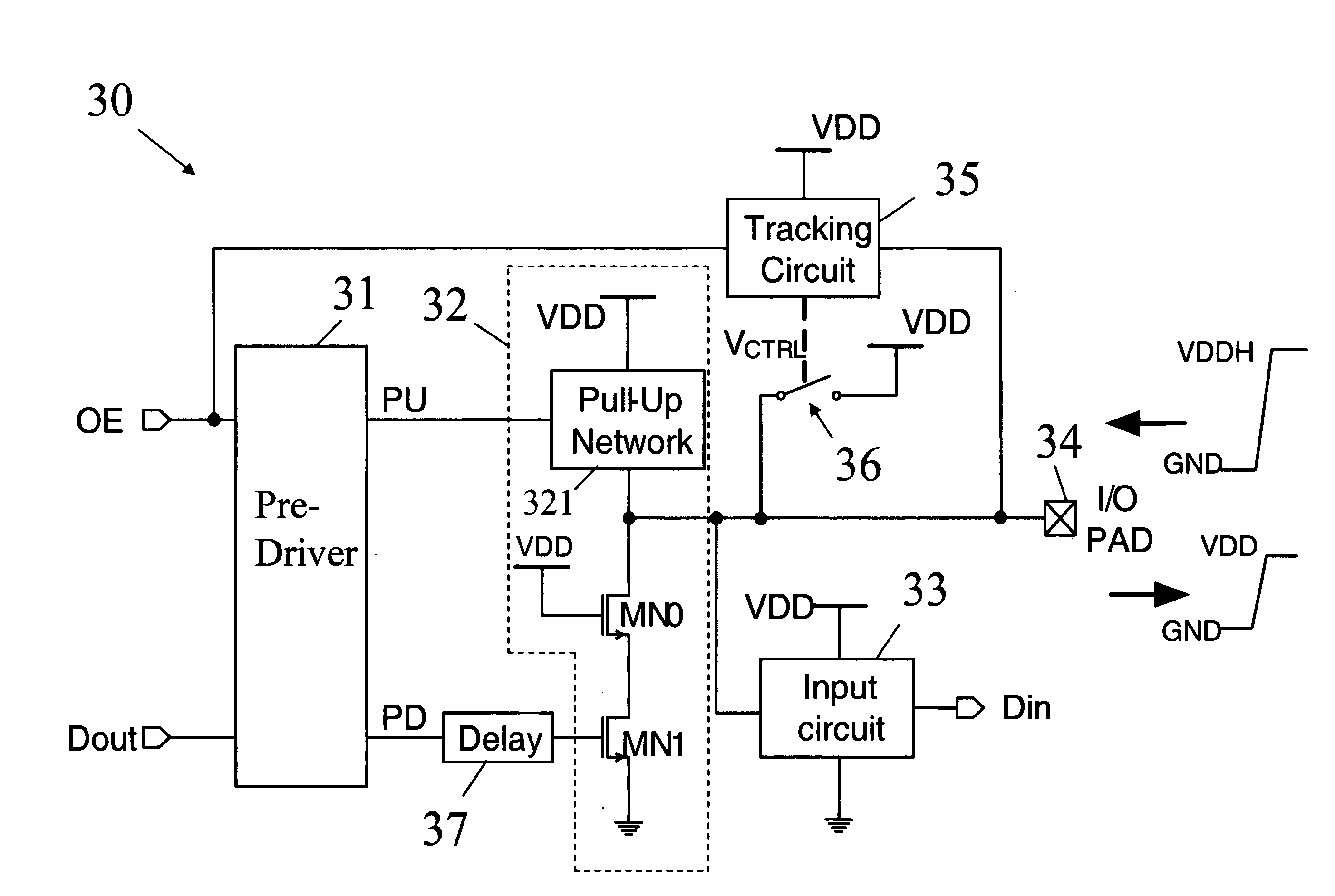
[0026]FIG. 3A is a schematic block diagram of a buffer circuit 30 in a mixed-voltage interface consistent with an example of the present invention. Referring to FIG. 3A, the buffer circuit 30 may include a pre-driver 31, a post-driver or output circuit 32, an input circuit 33, an input / output (I / O) pad 34, a tracking circuit 35 and a switch device 36. The post-driver 32 may further include a pull-up network 321 and stacked NMOS transistors MN0 and MN1. The pre-driver 31, the pull-up network 321 and the input circuit 33 are simplified into function blocks for convenience. The pre-driver 31 generates control signals PU and PD in response to an output enable (OE) signal and a data output (Dout) signal from an internal circu...


PUM


Abstract

A circuit configured for providing hot-carrier effect protection, the circuit comprising a first transistor including a first terminal and a second terminal, the first terminal being coupled to a conductive pad, a switch device including a terminal coupled to the conductive pad, and a control circuit configured for keeping the switch at an off state during a receiving mode at which a signal of a first voltage level or a reference level is received at the conductive pad, keeping the switch at the off state during a transmitting mode from which a signal of a second voltage level or the reference level is transmitted at the conductive pad, and keeping the switch at an on state during a transition from the receiving mode when receiving a signal of the first voltage level to the transmitting mode when transmitting a signal having the reference voltage level, wherein during the transition a voltage across the first terminal and the second terminal of the first transistor is maintained at a level below approximately the first voltage level minus the second voltage level.

Description

CROSS-REFERENCE TO RELATED APPLICATIONS[0001]This application claims the benefit of U.S. Provisional Application No. 60 / 823,453, filed Oct. 6, 2006.BACKGROUND OF THE INVENTION[0002]The present invention relates generally to circuits and methods for protecting a circuit or buffer, and more particularly, to a circuit configured for preventing the hot-carrier effect in a mixed-voltage input / output (I / O) buffers.[0003]With the progress in complementary metal-oxide-semiconductor (CMOS) manufacturing technologies, the dimensions of transistors have been scaled down to reduce the silicon cost as well as to meet the increasing demands for more reliable circuit performance and faster operating speed. The thinner gate oxide of a CMOS transistor helps reduce the core power supply voltage (VDD) and therefore achieves lower power consumption. However, the maximum tolerable voltage across the transistor terminals (drain, source, gate and bulk) should be decreased accordingly to ensure the lifetim...

Claims


Application Information

Patent Timeline
Patent Type & Authority Applications(United States)
IPC IPC(8): H03K19/094
CPCH03K19/094H03K19/00361
Inventor HU, FANG-LINGKER, MING-DOU
Owner IND TECH RES INST
Why Eureka
Try Eureka