Flash multi-level threshold distribution scheme

Active Publication Date: 2008-03-13
CONVERSANT INTPROP MANAGEMENT INC
View PDF43 Cites 62 Cited by
  • Summary
  • Abstract
  • Description
  • Claims
  • Application Information

AI Technical Summary

Benefits of technology

[0027]It is an object of the present invention to obviate or mitigate at least one disadvantage of previous multi-level Flash memory cells devices. For

Problems solved by technology

In PDA's, mass storage is required for storing applications and data, while portable music players and digital cameras require large amounts of mass storage for retaining music file data and/or image data.
This limits the selection to non-volatile forms of memory since volatile memories, such as static random access memory (SRAM) and dynamic random access memory (DRAM), require a constant application of power in order to retain data.
Variations in fabrication processes and ageing of the device may cause shifts in the threshold voltages.
These shifts can weaken the strength of cell states by moving one state closer to the next state.
A problem with this scheme is the required tightness of the distribution for each state and the distance between the states.
As a result, there is a potential that erased memory cells will have their threshold voltages unintentionally shifted.
This problem is more pronounced in multi-level cells as more levels are squeezed into a fixed voltage range.
This reduces read sensing margin and eventually leads to a failure to sense neighboring cell states.
In other words, Vt overlap or even minimum Vt distance between neighboring cell states leads to device failure.
However, for optimum performance of the memory cell, a lower Vread is preferred as high Vread can cause disturbance.
Furthermore, as the number of rewrite (erase & program) cycle increases

Method used


Image

  • Flash multi-level threshold distribution scheme
  • Flash multi-level threshold distribution scheme
  • Flash multi-level threshold distribution scheme

Examples


Example

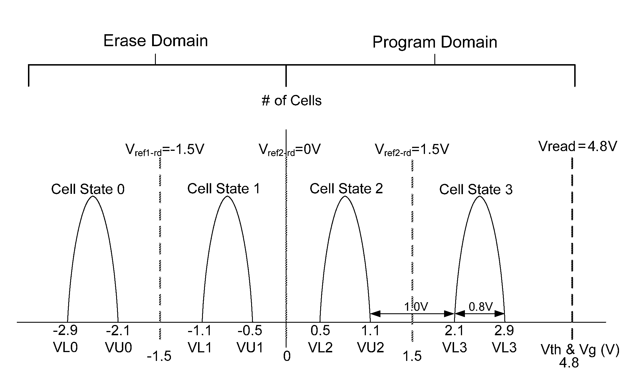
[0055]Generally, aspects of the present invention provide a threshold voltage distribution scheme for multi-level Flash cells with optimal Vt window and maximum Vt distance, while at the same time maintaining Vread at lower levels. In one embodiment, this is accomplished by programming at least one cell state in the erase voltage domain (for example, with a negative Vt value).

[0056]FIG. 7 is an exemplary embodiment of the invention. FIG. 7 shows a threshold voltage distribution for a multi-level Flash memory cell capable of storing 2 bits of data. In the present embodiment, there is one program state (cell state 1, corresponding to data “10”) lying in the erased voltage domain with erased state (cell state 0, corresponding to data “11”). Therefore, there are two cell states lying in the erased voltage domain and two cell states (cell state 2, corresponding to data “01” and cell state 3, corresponding to data “00”) in the program voltage domain. By programming this state in the erase...


PUM


Abstract

A threshold voltage distribution scheme for multi-level Flash cells where an erase threshold voltage and at least one programmed threshold voltage lie in an erase voltage domain. Having at least one programmed threshold voltage in the erase voltage domain reduces the Vread voltage level to minimize read disturb effects, while extending the life span of the multi-level Flash cells as the threshold voltage distance between programmed states is maximized. The erase voltage domain can be less than 0V while a program voltage domain is greater than 0V. Accordingly, circuits for program verifying and reading multi-level Flash cells having a programmed threshold voltage in the erase voltage domain and the program voltage domain use negative and positive high voltages.

Description

CROSS REFERENCE TO RELATED APPLICATIONS[0001]This application claims the benefit of priority of U.S. Provisional Patent Application No. 60 / 844,154 filed on Sep. 13, 2006 which is incorporated herein by reference in its entirety.FIELD OF THE INVENTION[0002]The present invention relates generally to Flash memory. More particularly, the present invention relates to a Flash memory device, a method for programming of Flash memory cell and a method for and a method for verifying a threshold voltage.BACKGROUND OF THE INVENTION[0003]Numerous types of consumer electronics products rely on some form of mass storage for retaining data or software for the execution of code by a microcontroller. Such consumer electronics are prolific, and include devices such as personal digital assistants (PDA's), portable music players, portable multimedia players (PMP's) and digital cameras. In PDA's, mass storage is required for storing applications and data, while portable music players and digital cameras ...

Claims


Application Information

Patent Timeline
IPC IPC(8): G11C16/04
CPCG11C11/5628G11C11/5642G11C16/0483G11C16/34G11C16/344G11C16/3454G11C2211/5621G11C16/12G11C16/14G11C16/10
Inventor KIM, JIN-KI
Owner CONVERSANT INTPROP MANAGEMENT INC
Why Eureka
Try Eureka