Conformal coatings for micro-optical elements

a technology of micro-optical elements and uniform coatings, which is applied in the direction of instruments, semiconductor lasers, transportation and packaging, etc., can solve the problems of element out of a specification range, functionality may be severely degraded, and the moe remains an emerging technology that has not yet developed a uniformly accepted nomenclature, etc., to achieve excellent surface conformance, sufficient thinness and precise

Inactive Publication Date: 2008-03-13
PLANAR SYSTEMS
View PDF1 Cites 36 Cited by
  • Summary
  • Abstract
  • Description
  • Claims
  • Application Information

AI Technical Summary

Benefits of technology

[0023] The final film thickness is controlled by the number of deposition cycles. Self-limiting growth provides excellent surface conformance and allows coatings on high aspect ratio structures and subwavelength structures. The present invention provides films that are sufficiently thin and precise for practical applications for MOEs. Furthermore, the resulting films are pinhole free, which is necessary for functionality in certain applications.

Problems solved by technology

MOEs are still an emerging technology that has not yet developed a uniformly accepted nomenclature.
Otherwise, the functionality may be severely degraded, or the element may be out of a specification range.
In particular, MOEs with structures having dimensions smaller than the wavelength of light are difficult structures on which to apply conformal coatings of uniform thickness.
Fabrication is further complicated where such structures have high aspect ratios.
However, these conventional techniques are not able to provide conformal coatings with uniform thickness for a subwavelength structure.
When coating material arrives on a substrate, its energy does not allow extended movement on the substrate surface.
This problem is pronounced where a subwavelength structure is involved.
However, the shadowed region will not be fully eliminated.
Furthermore, because PVD is based on flying material, there is always a “line of sight” problem so that sides of walls are difficult to coat.
In case of high aspect ratio, good step coverage is impossible.
CVD methods have difficulties in applying very thin films because the film does not always conform.
This is, however, practical only in applications having shallow steps and low aspect ratios.
Difficulties arise with conventional techniques, such as CVD, in having a film 64 conform to the deep trench 62.

Method used


Image

  • Conformal coatings for micro-optical elements
  • Conformal coatings for micro-optical elements
  • Conformal coatings for micro-optical elements

Examples


Embodiment Construction

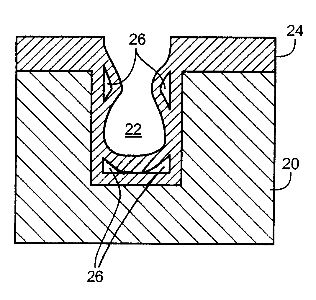
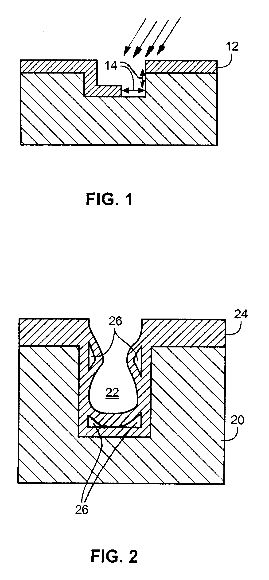
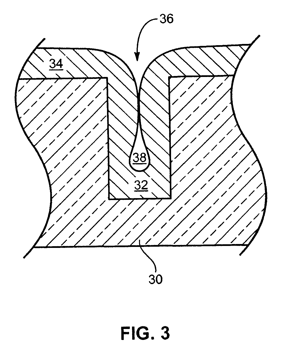
[0040] Reference is now made to the figures in which like reference numerals refer to like elements. For clarity, the first digit or digits of a reference numeral indicates the figure number in which the corresponding element is first used.

[0041] Throughout the specification, reference to “one embodiment” or “an embodiment” means that a particular described feature, structure, or characteristic is included in at least one embodiment of the present invention. Thus, appearances of the phrases “in one embodiment” or “in an embodiment” in various places throughout this specification are not necessarily all referring to the same embodiment.

[0042] Furthermore, the described features, structures, or characteristics may be combined in any suitable manner in one or more embodiments. Those skilled in the art will recognize that the invention can be practiced without one or more of the specific details, or with other methods, components, materials, etc. In other instances, well-known structu...


PUM

PropertyMeasurementUnit
aspect ratioaaaaaaaaaa
pressureaaaaaaaaaa

Abstract

A micro-optical element is produced through vapor deposition techniques, such as atomic layer deposition. An optical structure having a surface with uneven structures is exposed to one or more precursor vapors to create a self-limiting film growth on the surface of the optical structure. The film thickness may be increased and controlled by subsequent exposures. The resulting film conforms to surface structures having varying complex dimensions.

Description

RELATED APPLICATIONS [0001] This application claims priority to U.S. patent application Ser. No. 10 / 404,928 filed on Mar. 31, 2003, and entitled “Conformal Coatings for Micro-Optical Elements,” which is hereby incorporated by reference in its entirety.TECHNICAL FIELD [0002] The present invention relates to techniques for fabricating optical elements and, more specifically, to techniques for depositing thin films on optical elements having a surface with uneven structures. BACKGROUND OF THE INVENTION [0003] Micron-scale fabrication has enabled the development of micro-optical elements that are used in a variety of optical-electronic applications. A micro-optical element (MOE) offers compact, light-weight optics that can be mass-produced using low cost replication techniques. With the given trend towards miniaturization, these features are highly attractive. MOEs may be refractive, such as microlenses and microlens arrays, and bend or focus light according to geometric optics. MOEs ma...

Claims


Application Information

Patent Timeline
Patent Type & Authority Applications(United States)
IPC IPC(8): B05D3/10C23C16/44C23C16/455G02B1/10H01S5/028
CPCC23C16/45525C23C16/45555Y10T428/24612H01S5/028G02B1/10G02B1/113
Inventor MAULA, JARMO ILMARITORNQVIST, RUNAR OLOF IVAR
Owner PLANAR SYSTEMS
Why Eureka
Try Eureka