Semiconductor device and method of manufacturing the same

a technology of semiconductor devices and semiconductors, applied in the field of semiconductor devices, can solve problems such as the complicated manufacturing process of semiconductor devices

Active Publication Date: 2008-03-20
SOCIONEXT INC
View PDF5 Cites 44 Cited by
  • Summary
  • Abstract
  • Description
  • Claims
  • Application Information

AI Technical Summary

Benefits of technology

[0011] According to the present invention, the ballast resistor of the ESD protection element is formed of an impurity doped layer forming the extension regions of a first transistor including a first gate insulating film, and an impurity doped layer forming the extension region of a second transistor including a second gate insulating film thicker than the first gate insulating film, whereby no additional ion implantation step speciali...

Problems solved by technology

For this, a series of steps of forming the impurity doped l...

Method used


Image

  • Semiconductor device and method of manufacturing the same
  • Semiconductor device and method of manufacturing the same
  • Semiconductor device and method of manufacturing the same

Examples


first embodiment

A First Embodiment

[0023] The semiconductor device and the method of manufacturing the same according to a first embodiment of the present invention will be explained with reference to FIGS. 1 to 7B.

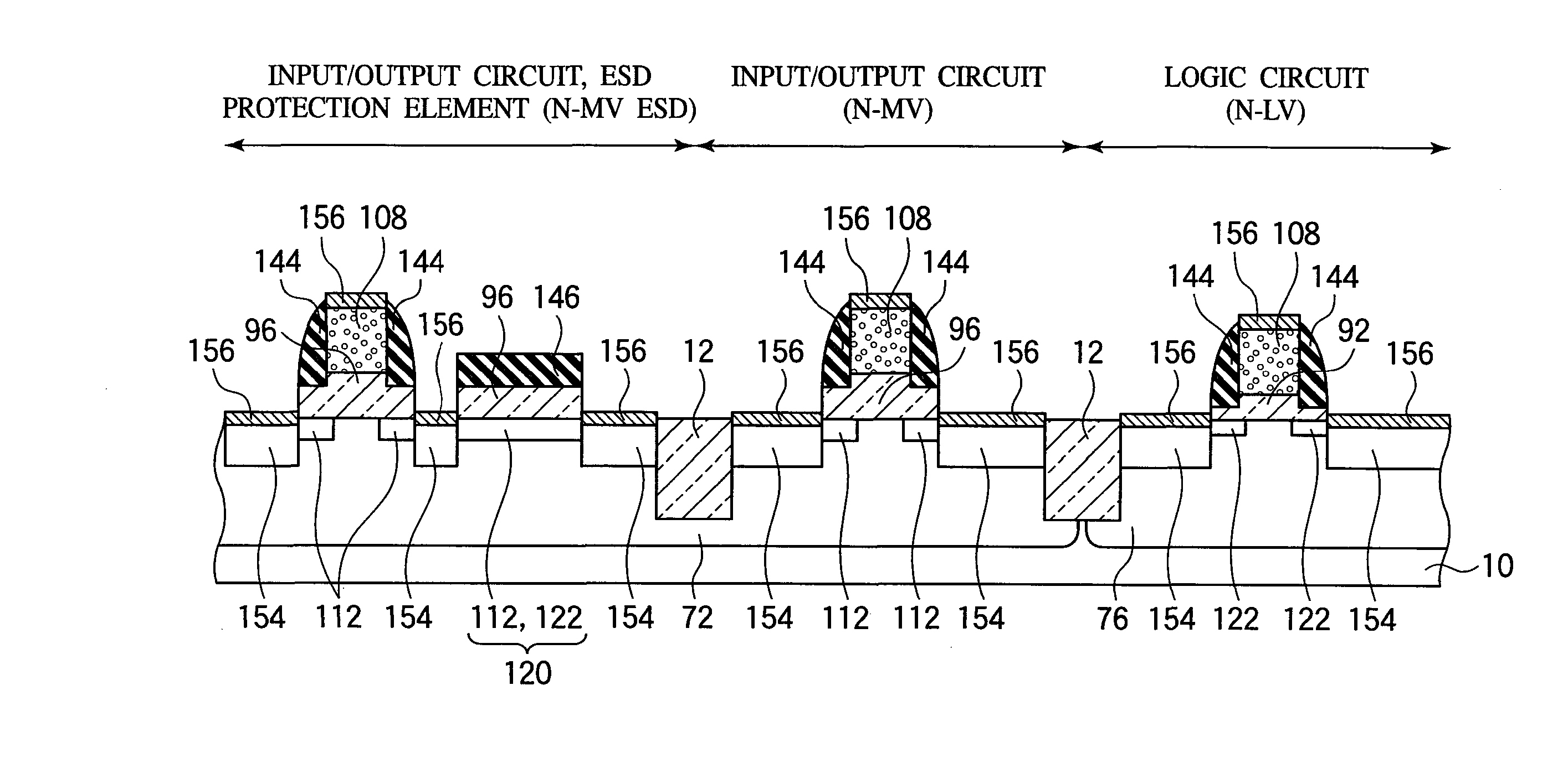
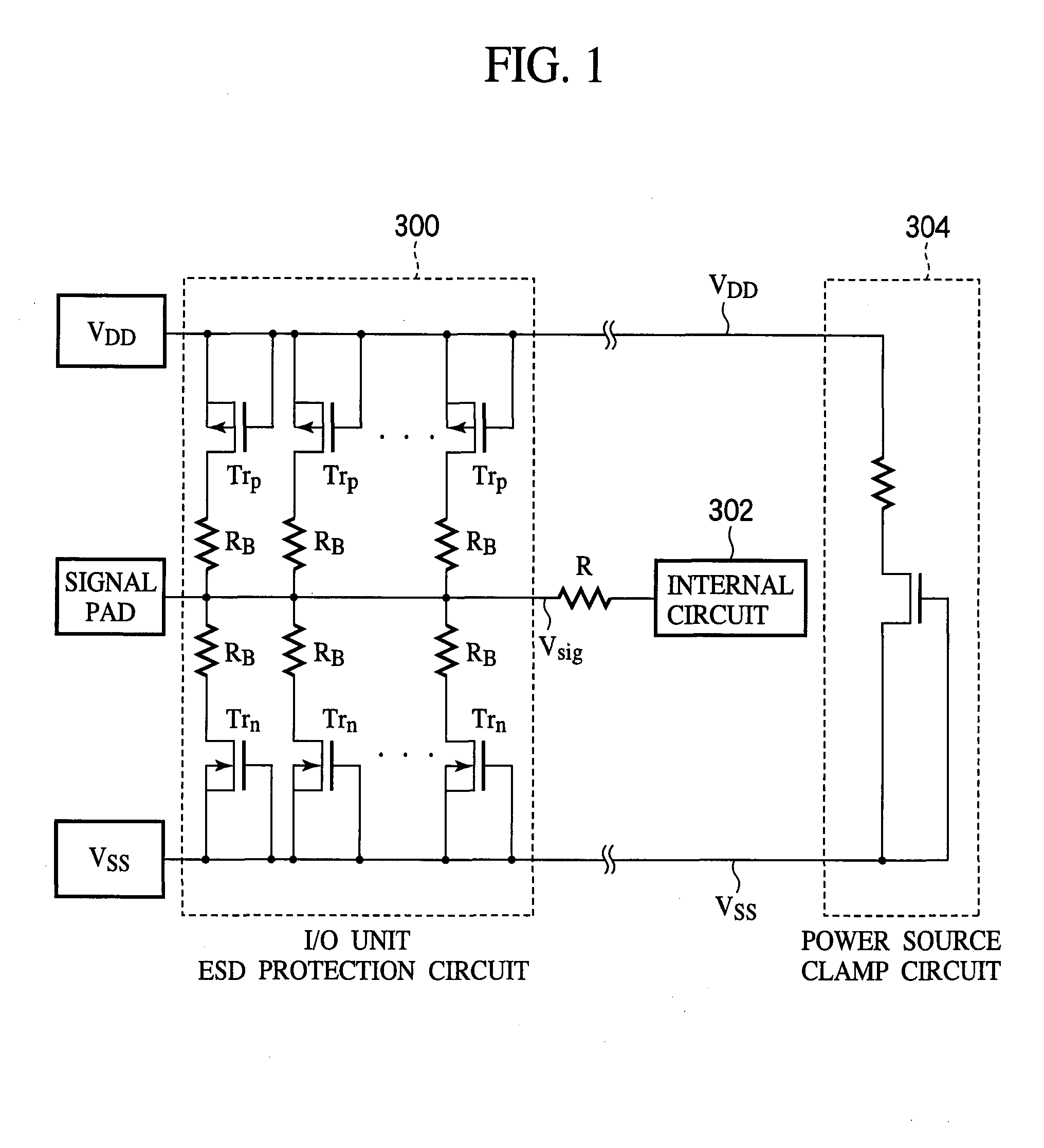
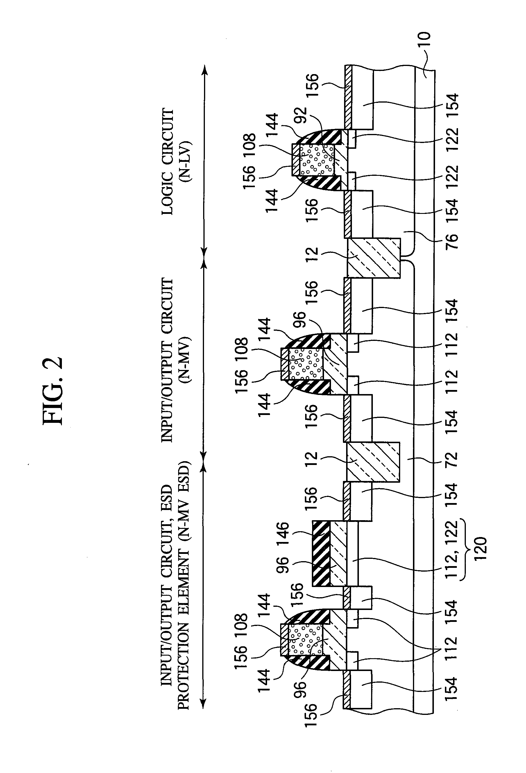
[0024]FIG. 1 is a circuit diagram of one example of the ESD protection circuit using MIS transistors including ballast resistors. FIG. 2 is a diagrammatic sectional view showing the structure of the semiconductor device according to the present embodiment. FIG. 3A-7B are sectional views showing the method of manufacturing the semiconductor device according to the present embodiment.

[0025] First, the ESD protection circuit using MIS transistors including ballast resistors will be explained with reference to FIG. 1. FIG. 1 shows one example of the ESD protection circuit of the I / O unit.

[0026] Between a VDD line and a signal line Vsig, a plurality of p-channel MIS transistors TrP each having a ballast resistor RB are parallelly connected. The p-channel MIS transistor TrP having the ballas...

second embodiment

A Second Embodiment

[0059] The semiconductor device and the method of manufacturing the same according to a second embodiment of the present invention will be explained with reference to FIGS. 8 to 21B. The same members of the present embodiment as those of the semiconductor device and the method of manufacturing the same according to the first embodiment shown in FIGS. 2 to 7B are represented by the same reference numbers not to repeat or to simplify their explanation.

[0060]FIG. 8 is a graph showing the depth-wise distribution of the impurity concentration of the extension region. FIG. 9 is a diagrammatic sectional view showing the structure of the semiconductor device according to the present embodiment. FIGS. 10A-20B are sectional views showing the method of manufacturing the semiconductor device according to the present embodiment. FIGS. 21A and 21B are views showing the effects of the semiconductor device and the method of manufacturing the same according to the present embodim...

third embodiment

A Third Embodiment

[0141] The semiconductor device and method of manufacturing the same according to a third embodiment of the present invention will be explained with reference to FIGS. 22 to 40B. The same members of the present embodiment as those of the semiconductor device and the method of manufacturing the same according to the first and the second embodiments are represented by the same reference numbers not to repeat or to simplify their explanation.

[0142]FIG. 22 is a diagrammatic sectional view showing the structure of the semiconductor device according to the present embodiment. FIGS. 23A to 40B are sectional views showing the method of manufacturing the semiconductor device according to the present embodiment.

[0143] In the present embodiment, the present invention is applied to a semiconductor combined with a flash memory.

[0144] First, the structure of the semiconductor device according to the present embodiment will be explained with reference to FIG. 22.

[0145] In a s...


PUM


Abstract

The semiconductor device includes a first MIS transistor including a gate insulating film 92, a gate electrode 108 formed on the gate insulating film 92 and source/drain regions 154, a second MIS transistor including a gate insulating film 96 thicker than the gate insulating film 92, a gate electrode 108 formed on the gate insulating film 96, source/drain regions 154 and a ballast resistor 120 connected to one of the source/drain regions 154, a salicide block insulating film 146 formed on the ballast resistor 120 with an insulating film 92 thinner than the gate insulating film 96 interposed therebetween, and a silicide film 156 formed on the source/drain regions 154.

Description

CROSS REFERENCE TO RELATED APPLICATIONS [0001] This application is a Continuation of International Application No. PCT / JP2005 / 009348, with an international filing date of May 23, 2005, which designating the United States of America, the entire contents of which are incorporated herein by reference.BACKGROUND OF THE INVENTION [0002] The present invention relates to a semiconductor device and a method of manufacturing the same, more specifically, a semiconductor device including an ESD protection element comprising a MIS transistor including a ballast resistor, and a method of manufacturing the semiconductor device. [0003] The semiconductor devices generally include ESD protection elements for protecting the semiconductor elements from voltage surges due to external ESD (ElectroStatic Discharge), etc. As an ESD protection element is known an ESD protection element using a MIS transistor having a ballast resistor, which functions also as an input / output circuit. Usually, in the MIS tra...

Claims


Application Information

Patent Timeline
IPC IPC(8): H01L23/62H01L21/336
CPCH01L21/823814H01L21/823857H01L27/0266H01L27/11546H01L27/105H01L27/11526H01L27/0629H10B41/49H10B41/40H01L21/8234H01L21/18H01L21/822
Inventor TSUTSUMI, TOMOHIKOEMA, TAIJIKOJIMA, HIDEYUKIANEZAKI, TORU
Owner SOCIONEXT INC
Why Eureka
Try Eureka