Wordline Booster Design Structure and Method of Operating a Wordline Booster Circuit

Inactive Publication Date: 2008-03-20
IBM CORP
View PDF1 Cites 5 Cited by
  • Summary
  • Abstract
  • Description
  • Claims
  • Application Information

AI Technical Summary

Benefits of technology

[0013]It is therefore an object of the invention to provide a design structure for a wordline booster circuit and which provides an improved read and write performanc

Problems solved by technology

The read and write performances of embedded SRAM arrays (SRAM=static random access memory) are a limiting factor for overall system speed.
Unfortunately, high supply voltages also cause undesirable high power dissipation.
The use of large SRAM cells, on the other hand, increases the costs because additional silicon area is needed on the chip, which is expensive and, therefore, undesired.
Using a separate supply voltage for the SRAM arrays causes high costs on the system side.
First, the voltage has to be generated, which causes costs for a voltage regulator.
Second, the voltage has to be distributed to the memory arrays, which causes costs on the packaging side.
Additionally, the array supply voltage must track with the surrounding logic supply voltage, in order to ensure ce

Method used


Image

  • Wordline Booster Design Structure and Method of Operating a Wordline Booster Circuit
  • Wordline Booster Design Structure and Method of Operating a Wordline Booster Circuit
  • Wordline Booster Design Structure and Method of Operating a Wordline Booster Circuit

Examples


Example

[0023]In the drawings identical elements or elements with identical functions are referred to with the same reference numeral.

DETAILED DESCRIPTION

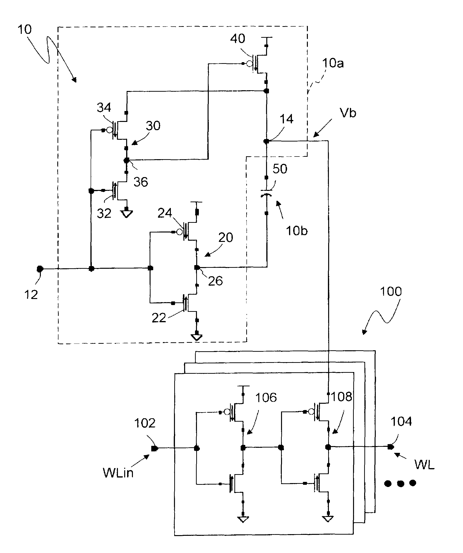
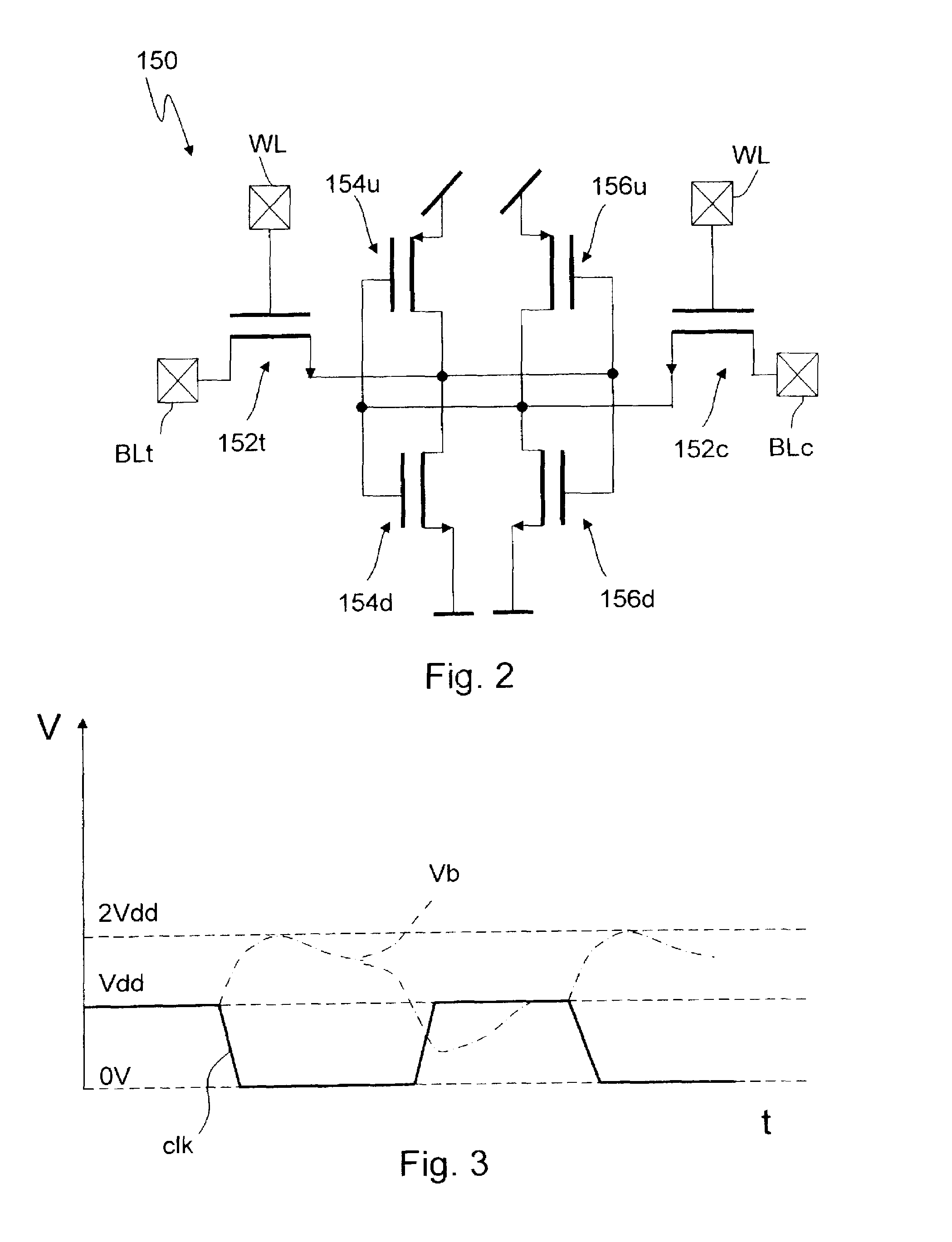
[0024]A wordline booster circuit is proposed which comprises a driving element for shifting a voltage level of a charge storage element for storing a charge necessary to generate a boosted voltage, a feedback element for controlling the switching state of a charging element, wherein the charging element is actively switchable between a turned-off state during a first time interval and a turned-on state during a second time interval, and an output port for supplying the boost voltage to at least one wordline-driver circuit of a memory device. The wordline booster circuit increases the voltage used for the wordline above the supply voltage level. Only the level for the wordline is increased. Preferably, the boosted output voltage of the circuit is supplied to all wordline-driver circuits. The boosted voltage is available at the negative edge...


PUM


Abstract

The invention relates to a wordline booster circuit, especially an SRAM-wordline booster circuit, comprising a driving element (20) for shifting a voltage level of a charge storage element (50) for storing a charge necessary to generate a boosted voltage (Vb), a feedback element (30) for controlling the switching state of a charging element (40), wherein the charging element (40) is actively switchable between a turned-off state during a first time interval and a turned-on state during a second time interval, and an output port (14) for supplying the boost voltage to at least one wordline-driver circuit (100) of a memory device (200). The invention relates also to an operation method for such a wordline booster circuit as well as a memory array implementation on an integrated circuit, especially an SRAM memory array, with a wordline booster circuit.

Description

CROSS REFERENCE TO RELATED APPLICATION[0001]This application is related to a European Patent Application No. 06120846.8, filed Sep. 18, 2006 and IBM Docket No. DE920060051US1 filed contemporaneously with this Application.FIELD OF THE INVENTION[0002]The invention relates to a design structure for a wordline booster circuit and a design structure for a memory-array with a wordline booster.[0003]The read and write performances of embedded SRAM arrays (SRAM=static random access memory) are a limiting factor for overall system speed. The performance is influenced by different factors, mainly the supply voltage and SRAM cell area.[0004]For high performance applications, large cells and / or high supply voltages are used to meet speed requirements.[0005]Unfortunately, high supply voltages also cause undesirable high power dissipation. Therefore separate voltages are used for SRAM cells and the surrounding logic to meet both, power and performance targets.[0006]The use of large SRAM cells, on...

Claims


Application Information

Patent Timeline
IPC IPC(8): G11C7/00
CPCG11C5/145G11C11/413G11C8/08
Inventor EHRENREICH, SEBASTIANPILLE, JUERGENTORREITER, OTTO
Owner IBM CORP
Why Eureka
Try Eureka