Electron-emitting device and manufacturing method thereof

a technology of electron-emitting film and manufacturing method, which is applied in the manufacture of electrode systems, electric discharge tubes/lamps, and screens, etc., can solve the problems that the above-mentioned conventional device using an electron-emitting film cannot always be realized in a state, and achieve high density, high resolution, and high-performance electron sources.

Inactive Publication Date: 2008-03-20
CANON KK
View PDF50 Cites 18 Cited by
  • Summary
  • Abstract
  • Description
  • Claims
  • Application Information

AI Technical Summary

Benefits of technology

[0016] Therefore, the present invention has been devised in order to solve the above-mentioned problems of the conventional art, and it is an object of the present invention to provide: a field emission electron-emitting device with which the spot size of an electron beam (electron beam diameter) is small, an electron-emitting area is large, highly efficient electron emission is possible with a low voltage, and a manufacturing process is easy; and an electron source and an image display apparatus utilizing such electron-emitting device.
[0053] According to the present invention described above, electron emission with a high density and stable of a current to be emitted in a low electric field can be obtained and, at the same time, an electron beam of high resolution can be realized. Moreover, an electron-emitting device exhibiting the above effects can be realized easily. Thus, in an electron source and an image display apparatus to which the electron-emitting device of the present invention is applied, a high performance electron source and image display apparatus can be obtained.

Problems solved by technology

However, the above-mentioned conventional device using an electron-emitting film cannot always be realized in a state in which the above-mentioned requirements can be satisfied simultaneously.

Method used


Image

  • Electron-emitting device and manufacturing method thereof
  • Electron-emitting device and manufacturing method thereof
  • Electron-emitting device and manufacturing method thereof

Examples


embodiments

[0147] Embodiments of the present invention will be hereinafter described in detail.

first embodiment

[0148] A manufacturing process of an electron-emitting device manufactured according to this embodiment will be described in detail using FIGS. 8A(a) to 8A(c).

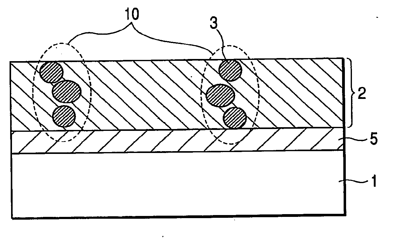
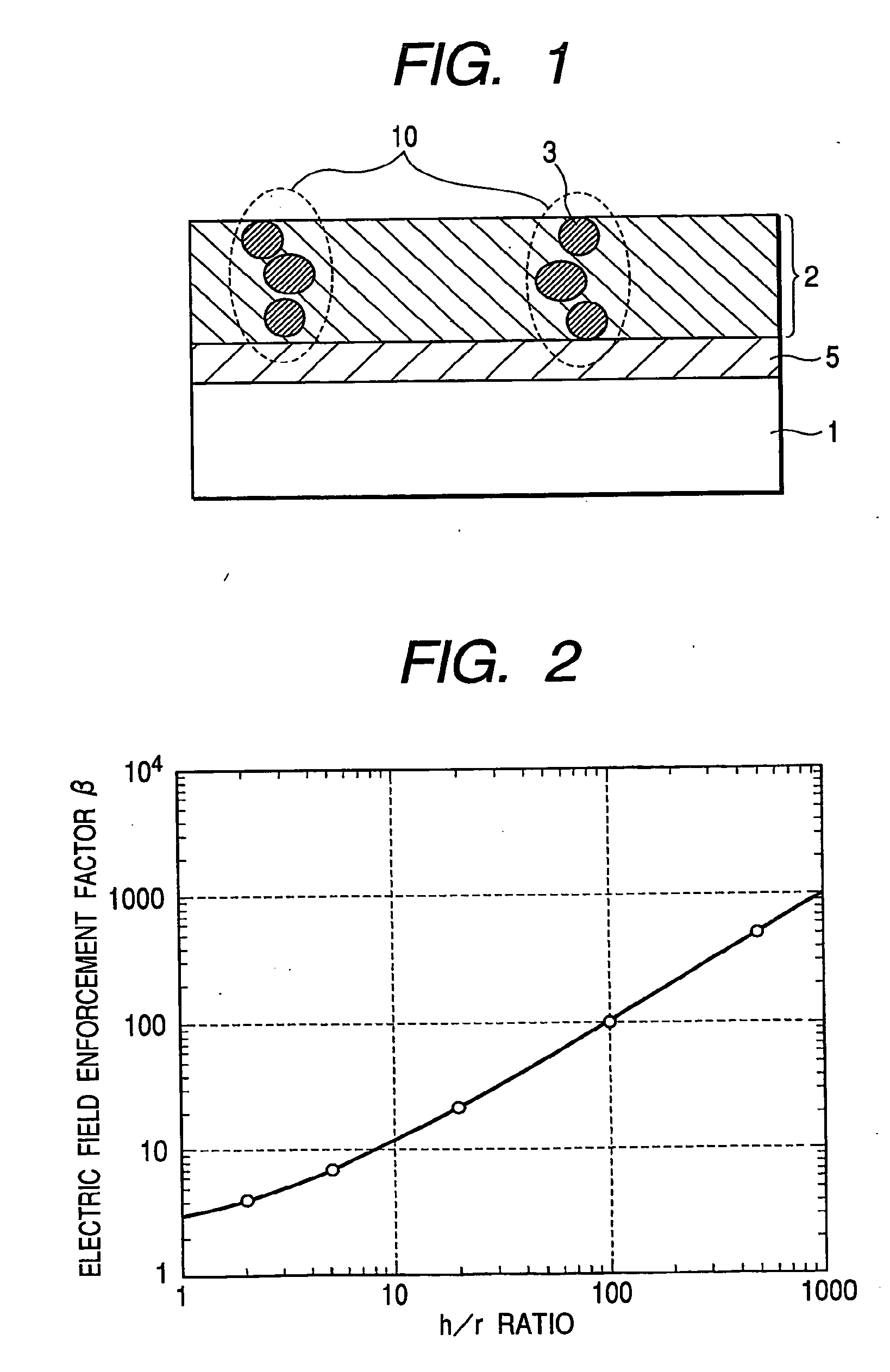
[0149] First, quartz was used as a substrate 1 and, after sufficiently cleaning the substrate, a film of Ta with a thickness of 500 nm was formed as a cathode electrode 5 by the sputtering method (FIG. 8A(a)).

[0150] Subsequently, a carbon film 2 with a nickel concentration of 0.02% was deposited to have a thickness of about 12 nm on the cathode electrode 5 by the sputtering method (FIG. 8A(b)). Ar was used as an atmospheric gas. Conditions are as described below: [0151] rf power supply: 13.56 MHz [0152] rf power: 400 W [0153] Gas pressure: 267 mPa [0154] Substrate temperature: 300° C. [0155] Target: Mixed target of graphite and nickel

[0156] Next, the substrate was subjected to heat treatment by lamp heating at 600° C. for 300 minutes in hydrogen containing atmosphere. Then, as shown in FIG. 8A(c), nickel cohered and a plura...

second embodiment

[0159] A manufacturing process of an electron-emitting device manufactured according to this embodiment will be described in detail using FIGS. 8B(a) to 8B(c).

[0160] First, quartz was used as a substrate 1 and, after sufficiently cleaning the substrate, a film of Ta with a thickness of 500 nm was formed as a cathode electrode 5 by the sputtering method (FIG. 8B(a)).

[0161] Subsequently, a carbon film 2 with a cobalt concentration of 0.3% and a hydrogen concentration of 1% was deposited to have a thickness of about 12 nm on the cathode electrode 5 by the sputtering method (FIG. 8B(b)). A mixed gas of Ar and H2 with a mixture ratio of 1:1 was used as an atmospheric gas.

Conditions are as described below:

[0162] rf power supply: 13.56 MHz [0163] graphite rf power: 1 KW [0164] cobalt rf power: 10 W [0165] Gas pressure: 267 mPa [0166] Substrate temperature: 300° C. [0167] Target: Mixed target of graphite and cobalt

[0168] Next, the substrate was subjected to heat treatment by lamp heat...


PUM

PropertyMeasurementUnit
temperatureaaaaaaaaaa
particle diameteraaaaaaaaaa
thicknessaaaaaaaaaa

Abstract

There is provided an electron-emitting device of a field emission type, with which the spot size of an electron beam is small, an electron emission area is large, highly efficient electron emission is possible with a low voltage, and the manufacturing process is easy. The electron-emitting device includes a layer 2 which is electrically connected to a cathode electrode 5, and a plurality of particles 3 which contains a material having a resistivity lower than that of a material constituting the layer 2, and is wherein a density of particles 3 in the layer 2 is 1×10¹⁴ / cm3 or more and 5×10¹⁸ / cm3 or less.

Description

RELATED APPLICATIONS [0001] This is a divisional of application Ser. No. 10 / 516,545, filed Dec. 2, 2004, which is the national phase of PCT / JP03 / 07544, filed Jun. 13, 2003, which in turn claims priority benefit under 35 U.S.C. §119 of Japanese patent applications 2002 / 172213, filed Jun. 13, 2002, and 2003 / 125030, filed Apr. 30, 2003. The entire disclosure of each of the mentioned applications is incorporated herein by reference.TECHNICAL FIELD [0002] The present invention relates to an electron-emitting device using an electron-emitting film, an electron source having a plurality of electron-emitting devices arranged therein, and an image display apparatus constituted by using the electron source. BACKGROUND ART [0003] In the case of applying an electron-emitting device using an electron-emitting film to an image display apparatus using phosphors, the electron-emitting device must produce an emission current sufficient for irradiating the phosphors with sufficient luminance. In addi...

Claims


Application Information

Patent Timeline
Patent Type & Authority Applications(United States)
IPC IPC(8): H01J9/02H01J1/304H01J29/04H01J31/12
CPCH01J9/025H01J1/3048H01J1/304B82Y40/00B82Y10/00H01J2201/30469H01J2201/30449
Inventor ICHIKAWA, TAKESHIFUJIWARA, RYOJISASAGURI, DAISUKE
Owner CANON KK
Why Eureka
Try Eureka