Yield-Enhancing Device Failure Analysis

a failure analysis and enhancing technology, applied in the direction of instruments, static storage, etc., can solve the problems of time-consuming and expensive process repeated, device failure, etc., and achieve the effect of increasing the manufacturing yield

Active Publication Date: 2008-03-20
TAHOE RES LTD
View PDF7 Cites 27 Cited by
  • Summary
  • Abstract
  • Description
  • Claims
  • Application Information

AI Technical Summary

Benefits of technology

[0005]The present invention, in illustrative embodiments thereof, comprises more efficient methods and apparatus for device failure analysis. For devices which include error correction circuitry therein, illustrative embodiments of the invention provide a means of increasing manufacturing yield by taking into account the error correction capabilities of a given device under test in determining whether or not the device passes a test series performed on the device.

Problems solved by technology

This time-consuming and expensive process would be repeated until each failed pattern was separately replicated, extracted, and analyzed.
Therefore, if the device fails a single test (i.e., if there is a single erroneous bit within the contents of a given address), the device is marked as failed.

Method used


Image

  • Yield-Enhancing Device Failure Analysis
  • Yield-Enhancing Device Failure Analysis
  • Yield-Enhancing Device Failure Analysis

Examples


Embodiment Construction

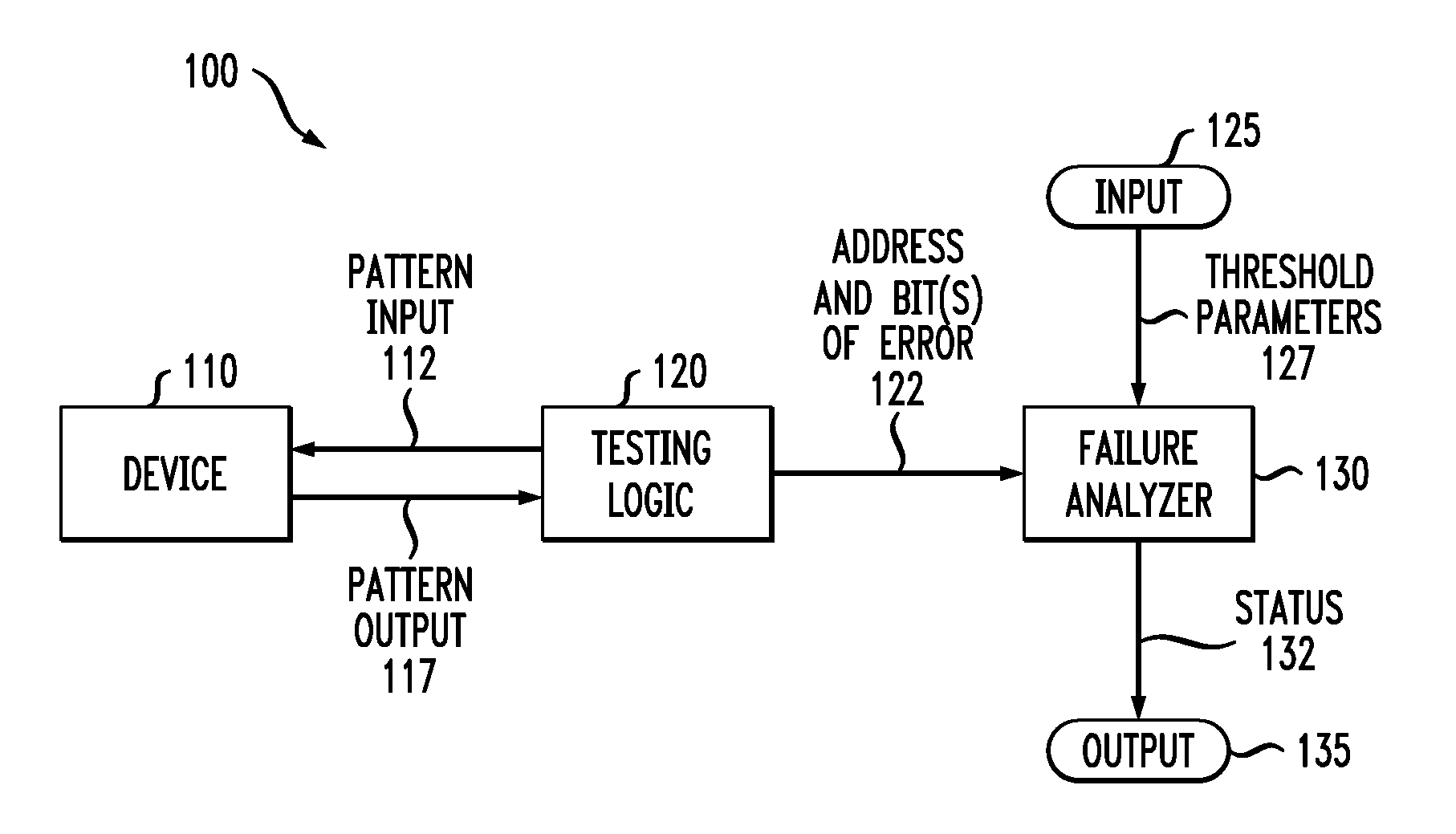
[0017]The present invention will be described herein in the context of exemplary methods and apparatus for improving failure analysis of electronic circuit devices including memory so as to increase a manufacturing yield of functioning devices. It is to be understood, however, that the techniques of the present invention are not limited to the methods and apparatus shown and described herein.

[0018]A “device” as the term is used herein may comprise, by way of example and without limitation, elements such as those commonly associated with an application-specific integrated circuit (ASIC), single inline memory module (SIMM), dual inline memory module (DIMM), content-addressable memory (CAM), central processing unit (CPU), digital signal processor (DSP), or any other type of data processing or storage device, as well as portions and / or combinations of such elements.

[0019]Although illustrated herein as comprising CAM, the invention does not require the use of CAM. Rather, techniques of i...


PUM


Abstract

In a system including a processor and memory coupled to the processor, a method of device failure analysis includes the steps of: upon each error detected within a test series performed on a device, the processor storing within a table in the memory an address at which the error occurred in the device and storing a bit position of each failed bit corresponding to that address; for each unique address at which at least one error occurred, determining how many different bit positions corresponding to the address failed during the test series; and based on results of the test series, determining whether the device failed the test series.

Description

FIELD OF THE INVENTION[0001]The present invention relates generally to techniques for electronic device testing, and more particularly relates to techniques for enhancing the yield of manufacturing such devices by means of improved failure analysis.BACKGROUND OF THE INVENTION[0002]As part of the manufacturing process, a device is tested by applying one or more test patterns (called a test series) to it and noting any unexpected results (errors). In cases where devices fail these tests by generating one or more errors and are not immediately discarded thereafter, these devices are then analyzed in a post-processing environment. That is, the device is put back on a tester and subjected to further testing, usually consisting of stepping through the original pattern sequence one pattern at a time until the error is replicated and then extracting internal status information from the chip for additional post-processing. This time-consuming and expensive process would be repeated until eac...

Claims


Application Information

Patent Timeline
Patent Type & Authority Applications(United States)
IPC IPC(8): G11C29/00
CPCG11C29/56G11C2029/5606G11C29/56008
Inventor BROWN, DAVID A.KIRK, JAMES THOMASSONNIER, DAVID P.STONE, CHRIS R.
Owner TAHOE RES LTD
Why Eureka
Try Eureka