III-V Hemt Devices

Active Publication Date: 2008-03-27
DENSO CORP
View PDF4 Cites 20 Cited by
  • Summary
  • Abstract
  • Description
  • Claims
  • Application Information

AI Technical Summary

Benefits of technology

[0059] In a semiconductor manufactured by the above method, it is easy to realize normally-off operation by depleting the upper layer and the second layer. It is consequently no longer necessary to maintain a high impurity concentration in the first layer so as to ensure stable normally-off operation, and a semiconductor device can be manufactured in which both stable

Problems solved by technology

However, in the semiconductor device described above, there is a problem that electrons in

Method used


Image

  • III-V Hemt Devices
  • III-V Hemt Devices
  • III-V Hemt Devices

Examples


Example

First Embodiment

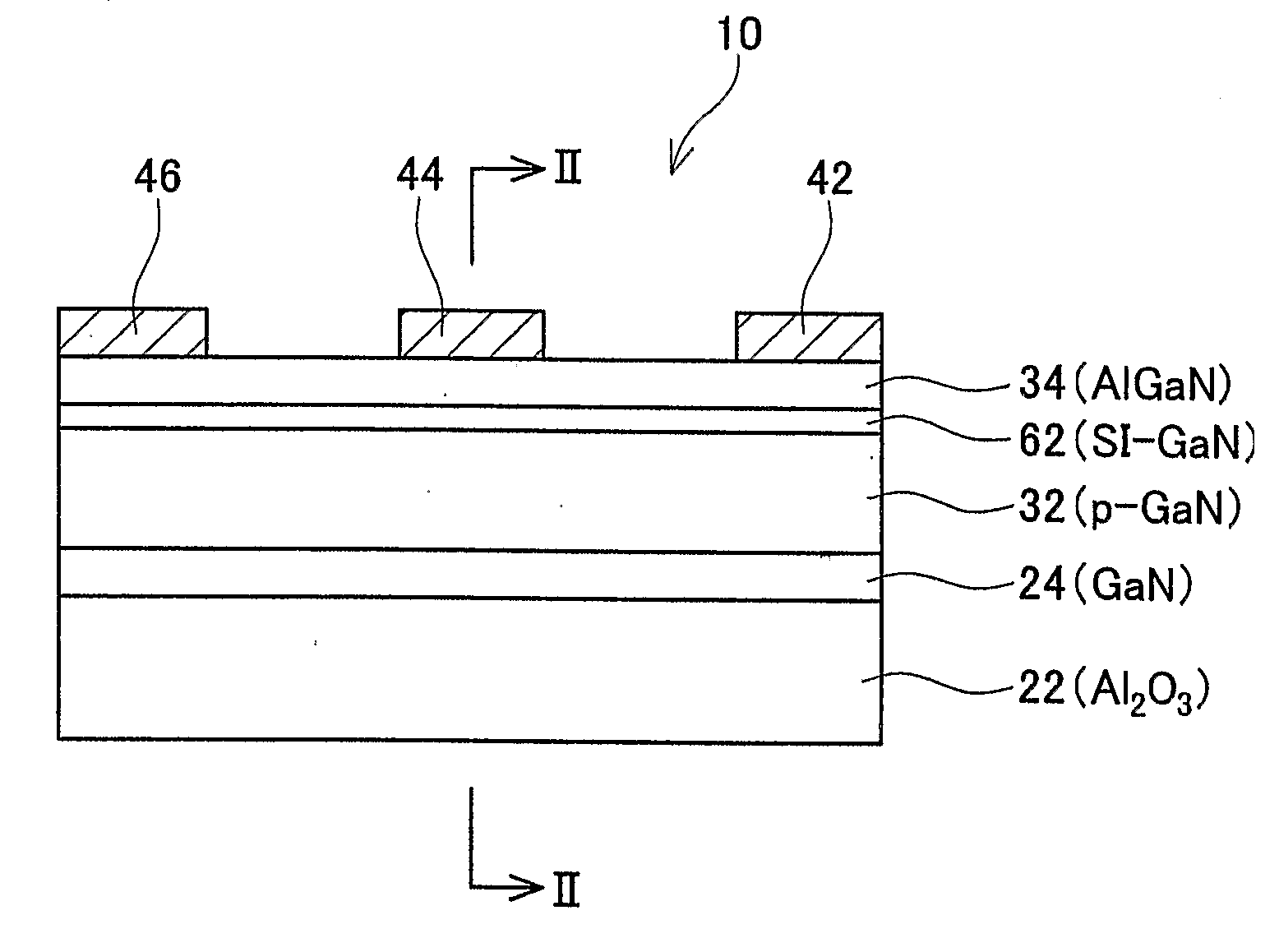
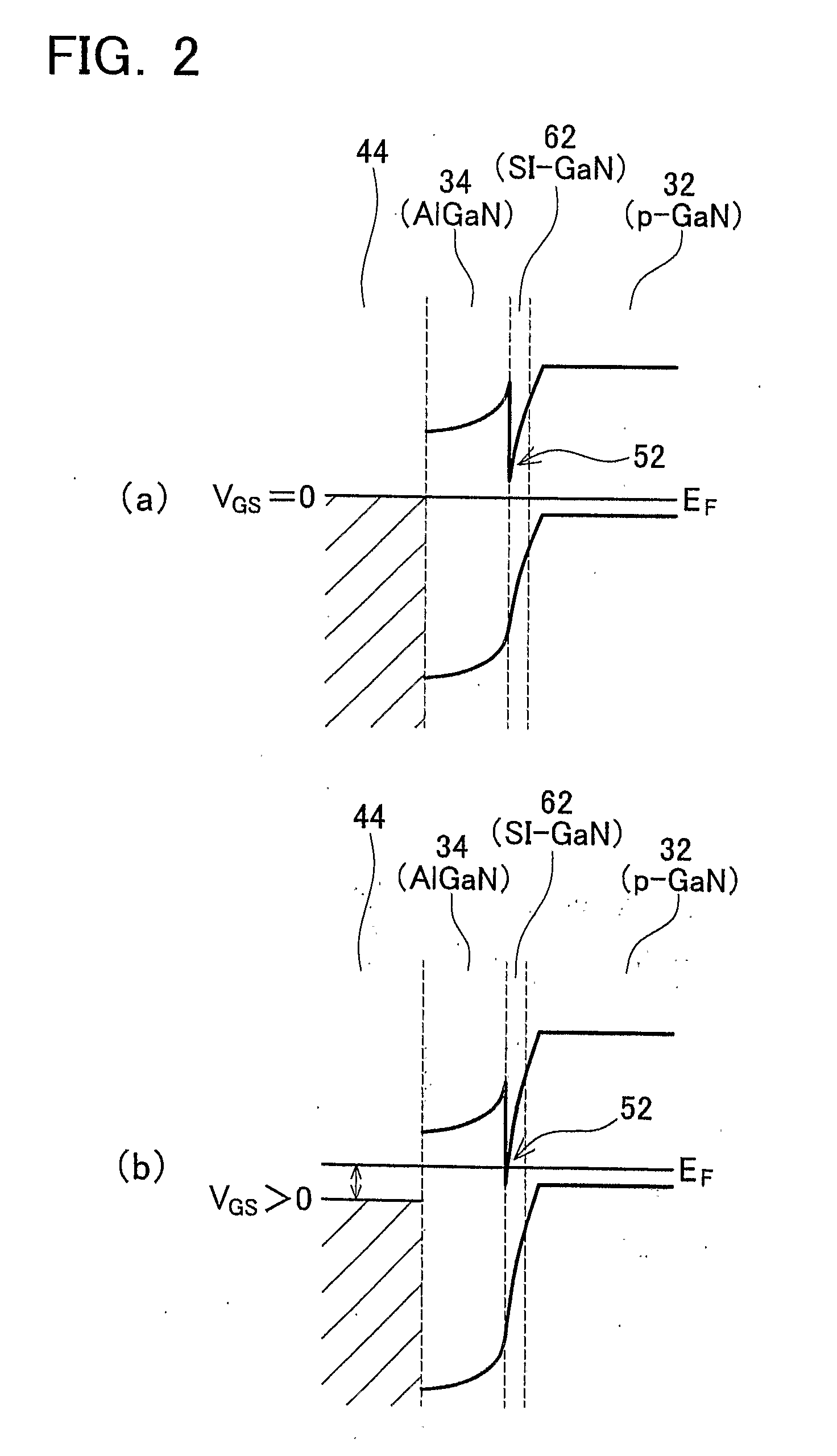
[0072]FIG. 1 schematically shows a cross-sectional view of essential parts of a semiconductor device 10 of the first embodiment.

[0073] The semiconductor device 10 comprises a substrate 22 formed from sapphire (Al2O3) at the bottom side. Instead of sapphire, silicon carbide (SiC), gallium nitride (GaN), etc. may be used to form the substrate 22. A buffer layer 24 formed from gallium nitride (GaN) is formed on the substrate 22. A p-GaN layer 32 (an example of a first layer), an SI (Semi Insulated)-GaN layer 62 (an example of a middle layer), and an AlGaN layer 34 (an example of a second layer), are stacked on the buffer layer 24.

[0074] The SI-GaN layer 62 is located between the p-GaN layer 32 and the AlGaN layer 34. The p-GaN layer 32 has been doped with magnesium (Mg). Semiconducting crystals of the AlGaN layer 34 contain aluminum (Al), and the AlGaN layer 34 has a wider band gap than the p-GaN layer 32 and the SI-GaN layer 62.

[0075] A gate electrode 44 (an exampl...

Example

Second Embodiment

[0094]FIG. 3 schematically shows a cross-sectional view of essential parts of a semiconductor device 100.

[0095] The semiconductor device 100 comprises a substrate 122 formed from sapphire (Al2O3) at the bottom side. Instead of sapphire, silicon carbide (SiC) or gallium nitride (GaN) may also be used to form the substrate 122. A buffer layer 124 formed from gallium nitride (GaN) is formed on the substrate 122. A GaN layer 132 (an example of a first layer), and an n-AlGaN layer 134 (an example of a second layer), are stacked on the buffer layer 124.

[0096] The n-AlGaN layer 134 has been doped with silicon (Si). Semiconducting crystals of the n-AlGaN layer 134 contain aluminum (Al), and the n-AlGaN layer 134 has a wider band gap than the GaN layer 132.

[0097] A gate electrode 144 (an example of an electrode) formed from a stacked structure of nickel (Ni) and gold (Au) is disposed at a center, relative to the page, of a top surface of the n-AlGaN layer 134. The gate e...

Example

Third Embodiment

[0113]FIG. 5 schematically shows a cross-sectional view of essential parts of a semiconductor device 200 of a third embodiment.

[0114] The semiconductor device 200 comprises a substrate 222 formed from sapphire (Al2O3) at a bottom side. Instead of sapphire, silicon carbide (SiC) or gallium nitride (GaN) may also be used to form the substrate 222. A buffer layer 224 formed from gallium nitride (GaN) is formed on the substrate 222. A p-GaN layer 232 (an example of a first layer), an n-AlGaN layer 233 (an example of a second layer), and a p-AlGaN layer 235 (an example of a surface layer), are stacked on the buffer layer 224.

[0115] The p-GaN layer 232 and the p-AlGaN layer 235 have been doped with magnesium (Mg). The n-AlGaN layer 233 has been doped with silicon (Si). Semiconducting crystals of the n-AlGaN layer 233 and the p-AlGaN layer 235 contain aluminum (Al), and the n-AlGaN layer 233 and the p-AlGaN layer 235 have a wider band gap than the p-GaN layer 232.

[0116]...


PUM


Abstract

The semiconductor device has a stacked structure in which a p-GaN layer 32, an SI-GaN layer 62, and an AlGaN layer 34 are stacked, and has a gate electrode 44 that is formed at a top surface side of the AlGaN layer 34. A band gap of the AlGaN layer 34 is wider than a band gap of the p-GaN layer 32 and the SI-GaN layer 62. Moreover, impurity concentration of the SI-GaN layer 62 is less than 1×1017 cm−3. The semiconductor devices comprising III-V semiconductors that have a stable normally-off operation are realized.

Description

[0001] The present application claims priority to Japanese Patent Application 2004-210989 filed on Jul. 20, 2004, the contents of which are hereby incorporated by reference. TECHNICAL FIELD [0002] This invention relates to normally-off type semiconductor devices comprising m-V semiconductors. BACKGROUND ART [0003] Since III-V semiconductors have a high breakdown field and a high saturated electron mobility, it is expected that semiconductor devices comprising III-V semiconductors will have a high breakdown voltage and will control large currents. Current research includes research on semiconductor devices that have a heterostructure comprising gallium nitride (GaN), an example of which is disclosed in Japanese Laid-Open Patent Application Publication No. 2003-59946. [0004] One of this type of semiconductor devices is an HEMT (High Electron Mobility Transistor) having a heterostructure comprising a p-GaN layer, and an n-AlGaN layer stacked on a top surface of the p-GaN layer. Since a...

Claims


Application Information

Patent Timeline
IPC IPC(8): H01L29/205H01L21/338H01L29/778H01L21/335H01L29/20H01L29/812
CPCH01L29/2003H01L29/66462H01L29/778H01L21/28H01L29/66431H01L29/7787
Inventor SUGIMOTO, MASAHIROKACHI, TETSUNAKANO, YOSHITAKAUESUGI, TSUTOMUUEDA, HIROYUKISOEJIMA, NARUMASA
Owner DENSO CORP
Why Eureka
Try Eureka