

Semiconductor device and method for manufacturing the same
a technology of semiconductors and semiconductors, applied in the direction of semiconductor devices, basic electric elements, electrical appliances, etc., can solve the problems of uniform silicide of silicon materials, and achieve the effects of easy control, large stress, and easy control
- Summary
- Abstract
- Description
- Claims
- Application Information
AI Technical Summary
Benefits of technology
Problems solved by technology
Method used
Image

Examples
first embodiment
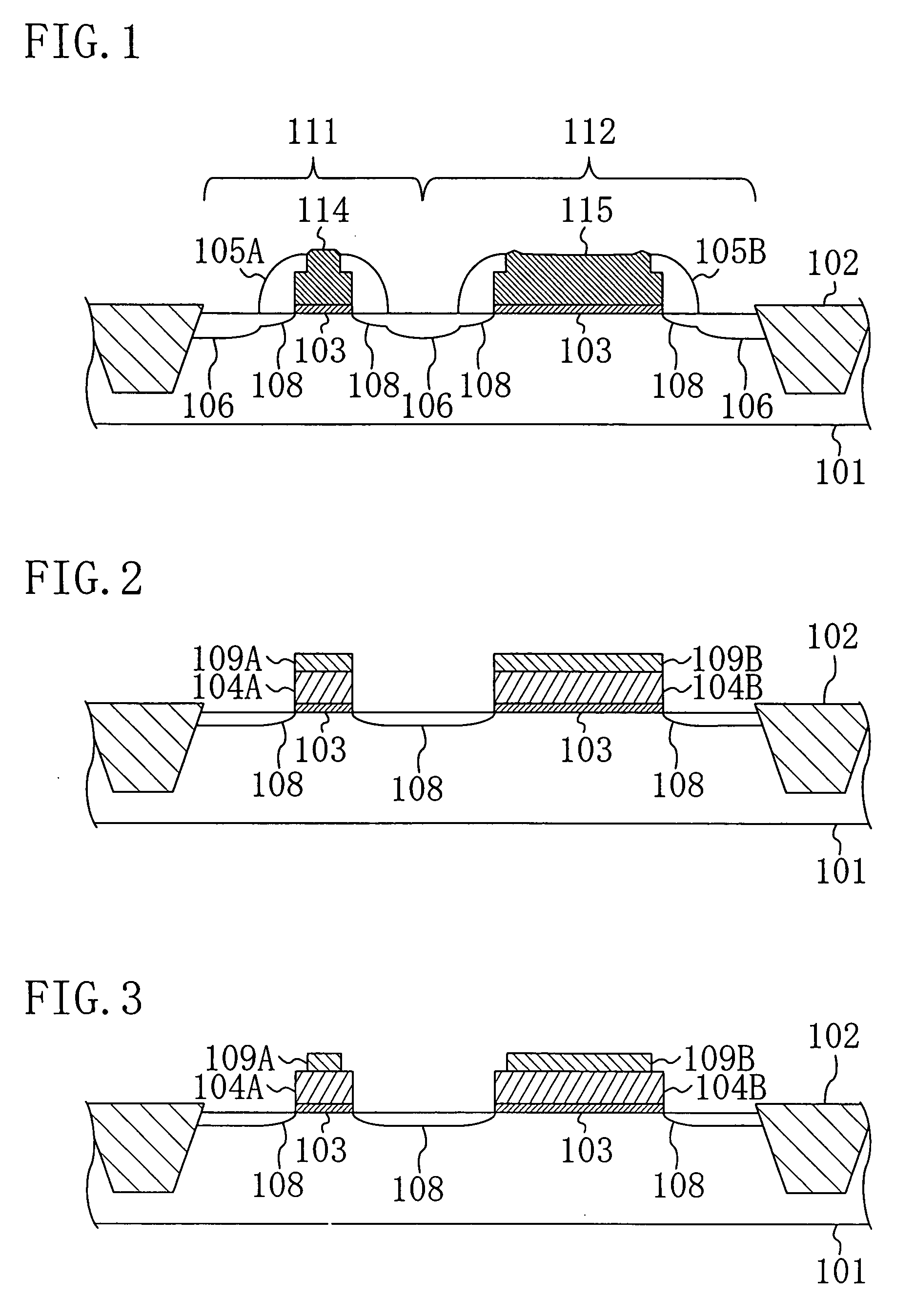
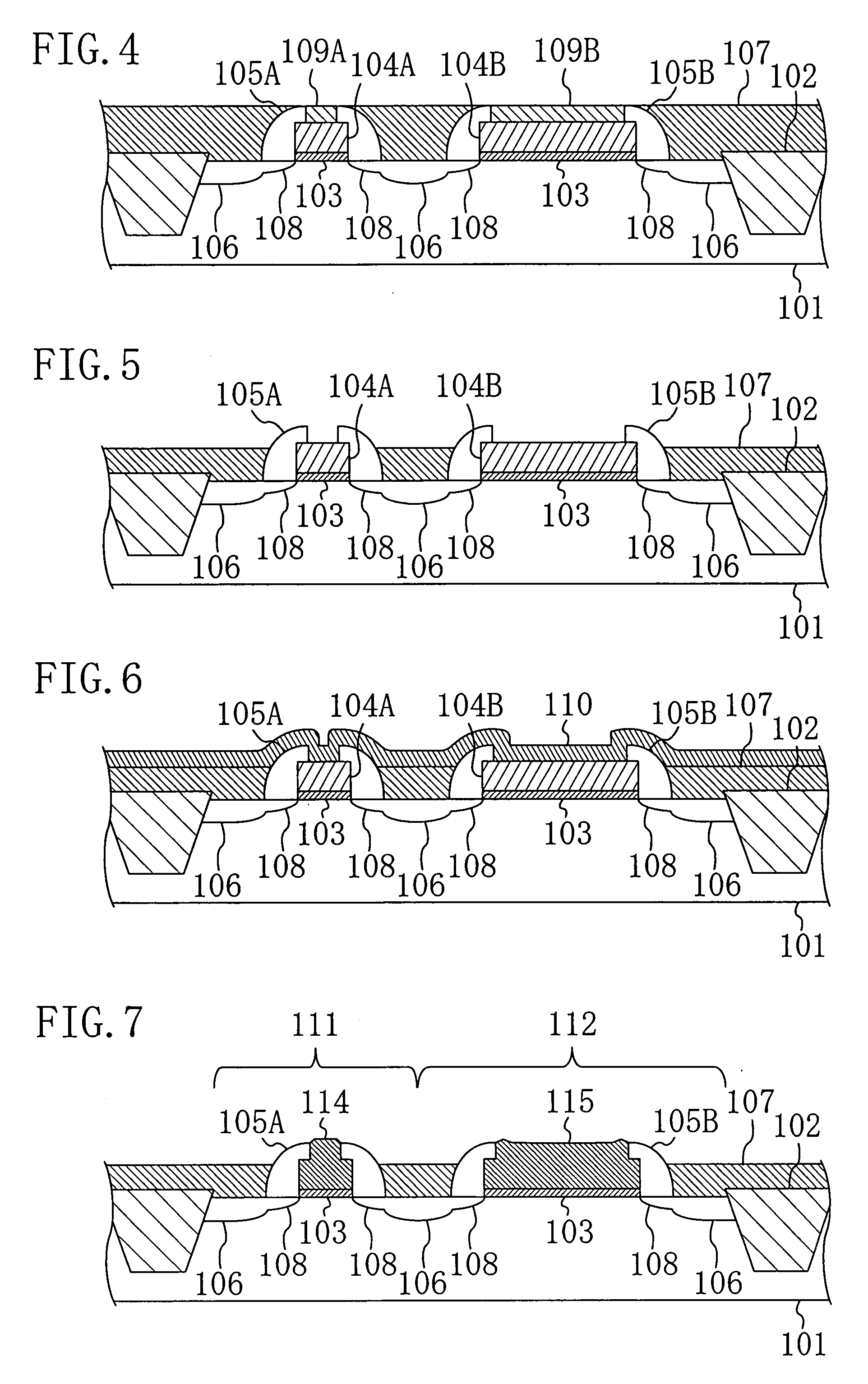
[0069]Hereinafter, explanation of a semiconductor device and a method for manufacturing the same according to a first embodiment of the present invention is provided with reference to the drawings. In the present embodiment, n-FETs are formed as a first FET Ill and a second FET 112.
[0070]FIG. 1 shows the sectional structure of the semiconductor device according to the present embodiment. As shown in FIG. 1, for example, an isolation region 102 is formed by a shallow trench isolation (STI) technique in the principal surface of a semiconductor substrate 101 made of silicon (Si) to define an active region and a region for forming a resistance element. In the present embodiment, a first FET 111 and a second FET 112 having different gate lengths are formed on the active region. More specifically, the first FET 111 includes a gate insulating film 103 formed on the active region of the semiconductor substrate 101, a first gate electrode 114 formed on the gate insulating film 103 and made o...
second embodiment
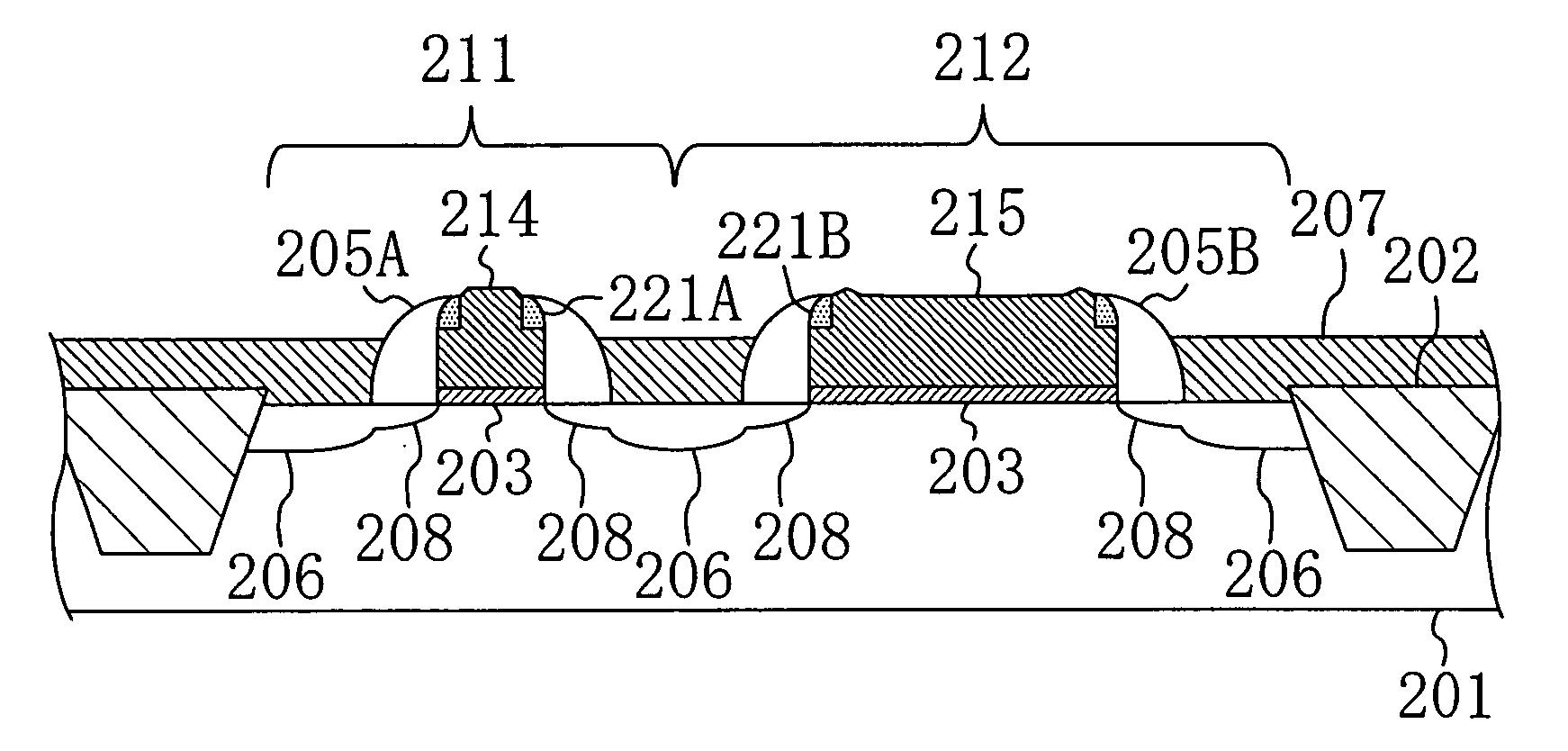
[0096]Hereinafter, explanation of a semiconductor device and a method for manufacturing the same according to a second embodiment of the present invention is provided with reference to the drawings. In the present embodiment, n-FETs are formed as a first FET 211 and a second FET 212.
[0097]FIG. 8 shows the sectional structure of a semiconductor device according to the present embodiment. As shown in FIG. 8, for example, an isolation region 202 is formed by a STI technique in the principal surface of a semiconductor substrate 201 made of silicon (Si) to define an active region and a region for forming a resistance element. In the present embodiment, a first FET 211 and a second FET 212 having different gate lengths are formed on the active region. More specifically, the first FET 211 includes a gate insulating film 203 formed on the active region of the semiconductor substrate 201, a first gate electrode 214 formed on the gate insulating film 203 and made of FUSI metal silicide, first...
third embodiment
[0127]Hereinafter, explanation of a semiconductor device and a method for manufacturing the same according to a third embodiment of the present invention is provided with reference to the drawings. In the present embodiment, n-FETs are formed as a first FET 311 and a second FET 312.
[0128]FIG. 17 shows the sectional structure of a semiconductor device according to the present embodiment. As shown in FIG. 17, for example, an isolation region 302 is formed by a STI technique in the principal surface of a semiconductor substrate 301 made of silicon (Si) to define an active region and a region for forming a resistance element. In the present embodiment, a first FET 311 and a second FET 312 having different gate lengths are formed on the active region. More specifically, the first FET 311 includes a gate insulating film 303 formed on the active region of the semiconductor substrate 301, a first gate electrode 314 formed on the gate insulating film 303 and made of FUSI metal silicide, firs...
PUM
 Abstract
Description
Claims
Application Information