Electrostatic discharge protection circuit
- Summary
- Abstract
- Description
- Claims
- Application Information
AI Technical Summary
Benefits of technology
Problems solved by technology
Method used
Image

Examples
Embodiment Construction
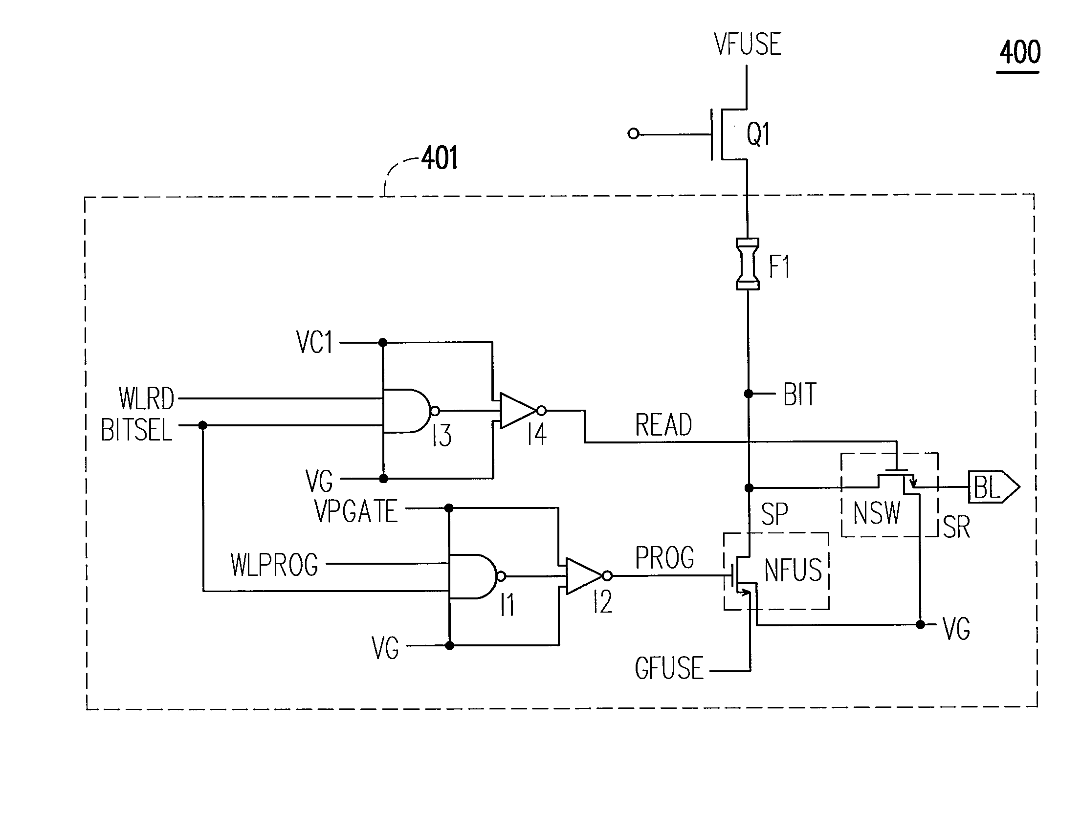
[0022]FIG. 4 illustrates an electrostatic discharge (ESD) protection circuit 400 according to an embodiment of the present invention. The ESD protection circuit 400 includes a fuse cell 401 and a metal oxide semiconductor field effect transistor (MOSFET) Q1. The fuse cell 401 contains a fuse F1 and outputs a bit data from its output terminal BL according to whether or not the fuse F1 is melted. The MOSFET Q1 is coupled between the fuse cell 401 and a voltage source VFUSE. The MOSFET Q1 is a MOSFET of large area and large size, and it is used for absorbing an ESD pulse from the voltage source VFUSE so that the ESD pulse would not melt the fuse F1. The MOSFET Q1 may be an n-channel or p-channel MOSFET.
[0023]The fuse cell 401 includes NAND gates I1 and I3, inverters I2 and I4, the fuse F1, a program switch SP, and a read switch SR. Wherein the material of the fuse F1 may be polysilicon or metal. The fuse F1 is coupled to the MOSFET Q1. The program switch is coupled between the fuse F1 ...
PUM
 Abstract
Description
Claims
Application Information