System and method for defect detection threshold determination in an workpiece surface inspection system

a technology of workpiece surface and threshold determination, which is applied in the direction of instruments, computing, measurement devices, etc., can solve the problems of variation in the false defect detection rate of the system, the possibility that an apparent defect detection actually constitutes a false identification of a defect, and the amount of reflected and scattered light of the same type of wafer from different manufacturers may be considerable, so as to achieve high sensitivity and reliability

Active Publication Date: 2008-03-27
KLA CORP
View PDF22 Cites 31 Cited by
  • Summary
  • Abstract
  • Description
  • Claims
  • Application Information

AI Technical Summary

Benefits of technology

[0019]Accordingly, an object of the present invention according to one aspect is to provide apparatus and methods for inspecting a surface of a workpiece with high sensitivity and reliability, e.g., for surface defects.
[0043]In a further embodiment, a method inspecting a surface of a semiconductor workpiece, the method comprises providing a surface inspection system and using the surface inspection apparatus to cause laser light to impinge upon a test location on the workpiece surface and thereby cause the laser light to emerge from the surface as returned light comprising at least one of reflected light and scatter light; collecting the returned light and generating a signal from the returned and collected light, the signal comprising a signal value representative of a characteristic of the workpiece surface at the test location; providing a plurality of threshold candidates in respective tiers and causing the surface inspection system to select a threshold from among the plurality of threshold candidates using the tiers; comparing the threshold to the signal value to obtain a difference value; using the difference value to assess the characteristic of the workpiece surface at the test location; and using the surface inspection system to automatically cause the method to be repeated for a plurality of test locations on the workpiece surface.

Problems solved by technology

A trade-off exists between the probability of defect detection and the reliability of defect detection in scattered light measurements.
However, as the threshold is set lower, the probability increases that an apparent defect detection actually constitutes a false identification of a defect, also known as a “false alarm”.
Further, even the same type of wafer from different manufacturers may have considerable differences in the amount of reflected and scattered light.
In a scenario in which the amount of reflected and scattered light is subject to change, use of a constant defect detection threshold will result in variation in a system's false defect detection rate, resulting in either identifying an increased number of false defects or failing to identify smaller defects that would otherwise have been reliably measurable.
In summary, a lack of confidence can develop in the ability of a surface inspection system to consistently detect defects.
However, false alarm thresholds may overload the measurement system with unnecessary data when the measured wafers are not of the highest quality, such as reclaim wafers.
This overload burdens the machine by slowing it down, and yields large sized wafer maps that have to be stored by the manufacturers.
Additional burdens include increases in storage needs, data transport and data management.
In practice, it is quite tedious to manually determine false detection rates and set optimal defect size-determined thresholds for every wafer type / batch in a production environment.

Method used


Image

  • System and method for defect detection threshold determination in an workpiece surface inspection system
  • System and method for defect detection threshold determination in an workpiece surface inspection system
  • System and method for defect detection threshold determination in an workpiece surface inspection system

Examples


Embodiment Construction

[0067]Reference will now be made in detail to presently preferred embodiments and methods of the invention as illustrated in the accompanying drawings, in which like reference characters designate like or corresponding parts throughout the drawings. It should be noted, however, that the invention in its broader aspects is not limited to the specific details, representative devices and methods, and illustrative examples shown and described in this section in connection with the preferred embodiments and methods. The invention according to its various aspects is particularly pointed out and distinctly claimed in the attached claims read in view of this specification, and appropriate equivalents.

Surface Inspection System

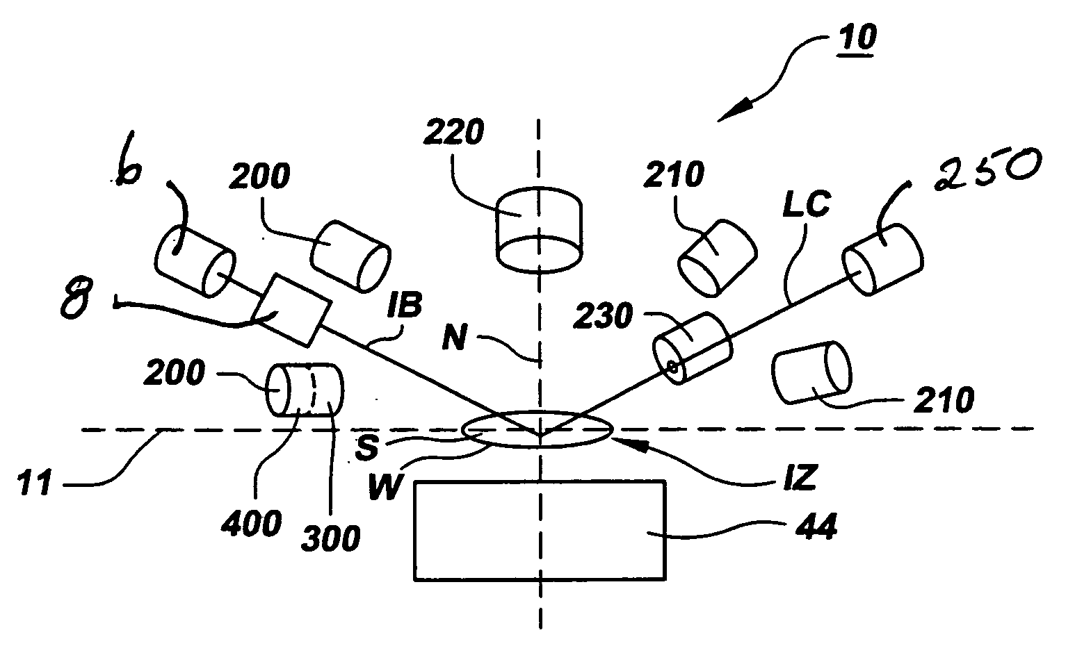
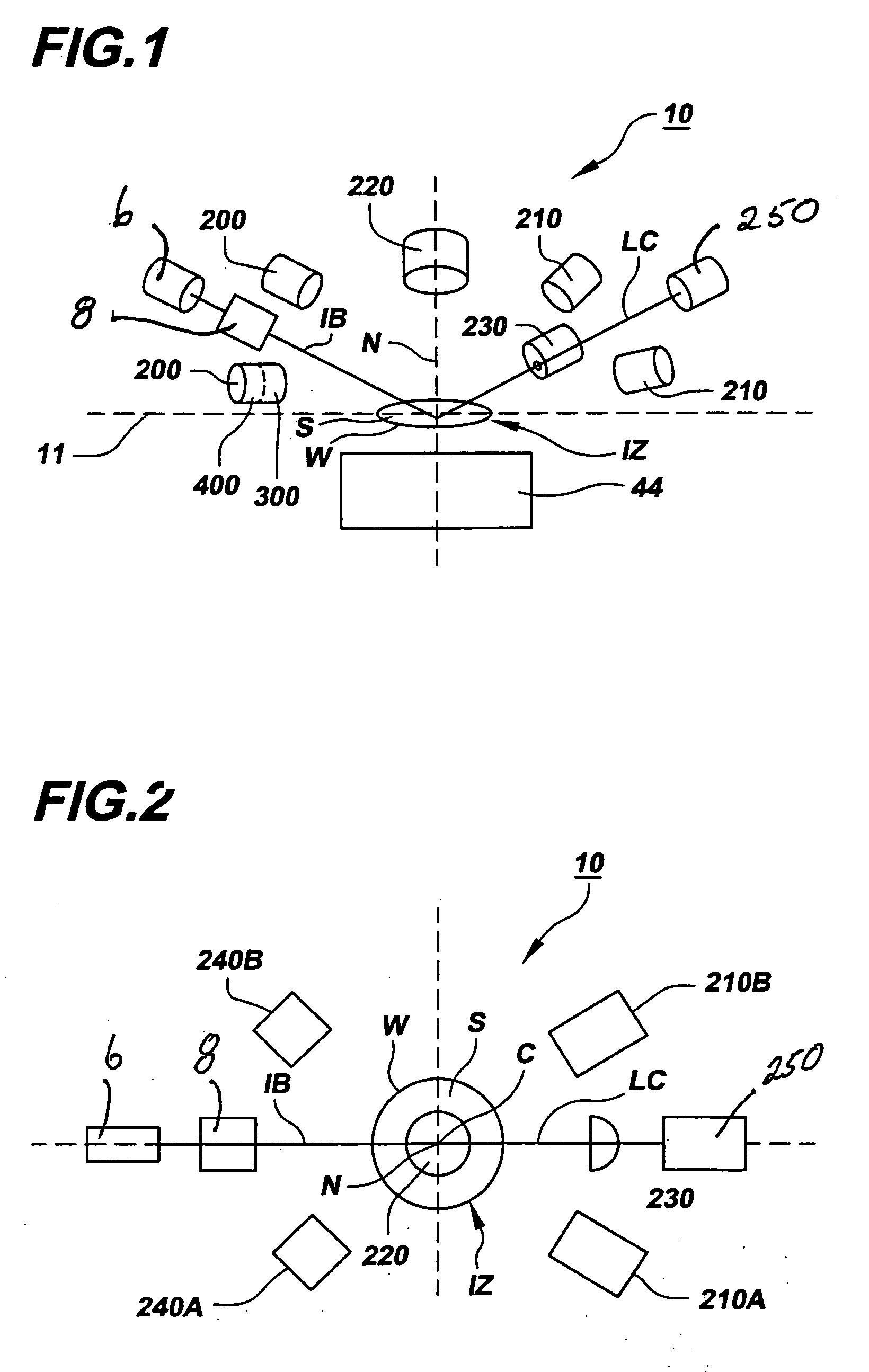
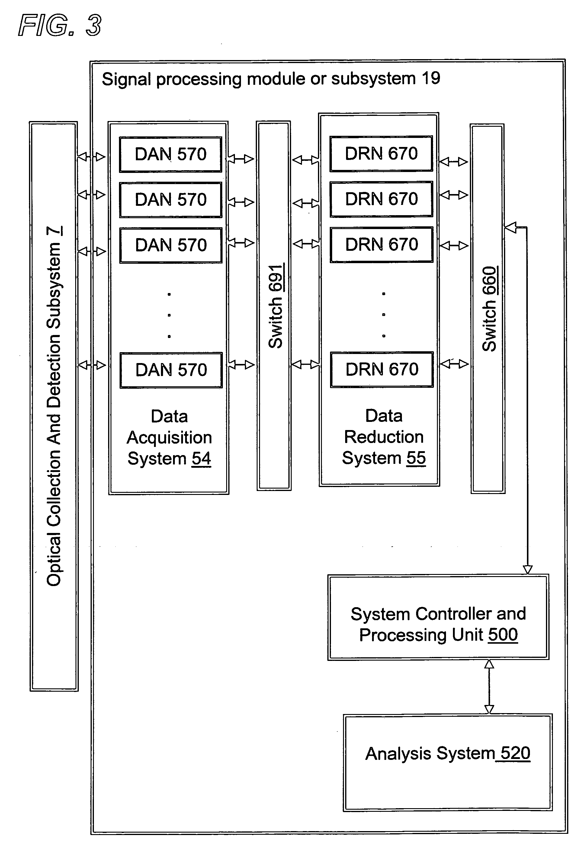
[0068]A surface inspection system 10 and related components, modules and subassemblies in accordance with a presently preferred embodiment of and method implementing the invention will now be described. Surface inspection system 10 is designed to inspect a surface S or ...


PUM


Abstract

A method and system for inspecting a surface of a semiconductor workpiece comprises providing a surface inspection system and using the surface inspection apparatus to cause laser light to impinge upon a test location on the workpiece surface and thereby cause the laser light to emerge from the surface as returned light comprising at least one of reflected light and scatter light; collecting the returned light and generating a signal from the returned and collected light, the signal comprising a signal value representative of a characteristic of the workpiece surface at the test location; providing a plurality of threshold candidates and causing the surface inspection system to select a threshold from among the plurality of threshold candidates; comparing the threshold to the signal value to obtain a difference value; using the difference value to assess the characteristic of the workpiece surface at the test location; and using the surface inspection system to automatically cause the method to be repeated for a plurality of test locations on the workpiece surface.

Description

BACKGROUND OF THE INVENTIONCross-Reference to Related Application[0001]N / ASTATEMENT REGARDING FEDERALLY SPONSORED RESEARCH OR DEVELOPMENT[0002]N / AFIELD OF THE INVENTION[0003]The present invention relates to technology for the inspection of a surface or surfaces of a workpiece, such as a semiconductor wafer, chip, or the like. More particularly, it relates to apparatus and methods for inspection of such workpiece surfaces using electromagnetic energy, e.g., light, to scan the surface to obtain characteristics of the surface or other information concerning the surface.DESCRIPTION OF THE RELATED ART[0004]There are a number of applications in which it is desirable or advantageous to inspect a surface or surfaces of a workpiece to obtain information about the characteristics and / or condition of that surface or surfaces. Examples of workpieces amenable to such application would include, for example, bare or unpatterned semiconductor wafers, semiconductor wafers with an applied film or fil...

Claims


Application Information

Patent Timeline
Patent Type & Authority Applications(United States)
IPC IPC(8): G06K9/00G06V10/145G06V10/30G06V10/98
CPCG01N21/4738G01N21/9501G01N2021/4711G01N2021/4735G06K9/6277G06K9/03G06K9/2036G06K9/40G01N2021/8861G06V10/98G06V10/145G06V10/30G06F18/2415
Inventor TEK, MEHMETTIEMEYER, TIMOTHYVERTIKOV, ANDREY
Owner KLA CORP
Why Eureka
Try Eureka