Semiconductor device having an epitaxial-grown contact plug

a technology of epitaxial growth and contact plug, which is applied in the direction of semiconductor devices, semiconductor/solid-state device details, electrical apparatus, etc., can solve the problems of short-channel effect of resultant mosfets, short-circuit failure between adjacent source regions, etc., and achieve the effect of suppressing short-circuit failure and reducing contact resistan

Inactive Publication Date: 2008-04-03
ELPIDA MEMORY INC
View PDF2 Cites 2 Cited by
  • Summary
  • Abstract
  • Description
  • Claims
  • Application Information

AI Technical Summary

Benefits of technology

[0009]In view of the above, it is an object of the present invention to provide a method for forming contact plugs on a silicon substrate, which is capable of suppressing the short-circuit failure between adjacent contact plugs and reducing the contact resistance between the contact plugs and the silicon substrate.

Problems solved by technology

However, a higher concentration of the impurities in the contact plugs may incur diffusion of the impurities doped in the contact plugs toward the silicon substrate during a later heat treatment, thereby causing a short-channel effect m the resultant MOSFETs.
This may incur a short-circuit failure between adjacent source regions 19 on the STI structure 12.

Method used


Image

  • Semiconductor device having an epitaxial-grown contact plug
  • Semiconductor device having an epitaxial-grown contact plug
  • Semiconductor device having an epitaxial-grown contact plug

Examples


Embodiment Construction

[0022]Now, an exemplary embodiment of the present invention will be described with reference to accompanying drawings, wherein similar constituent elements are designated by similar reference numerals throughout the drawings.

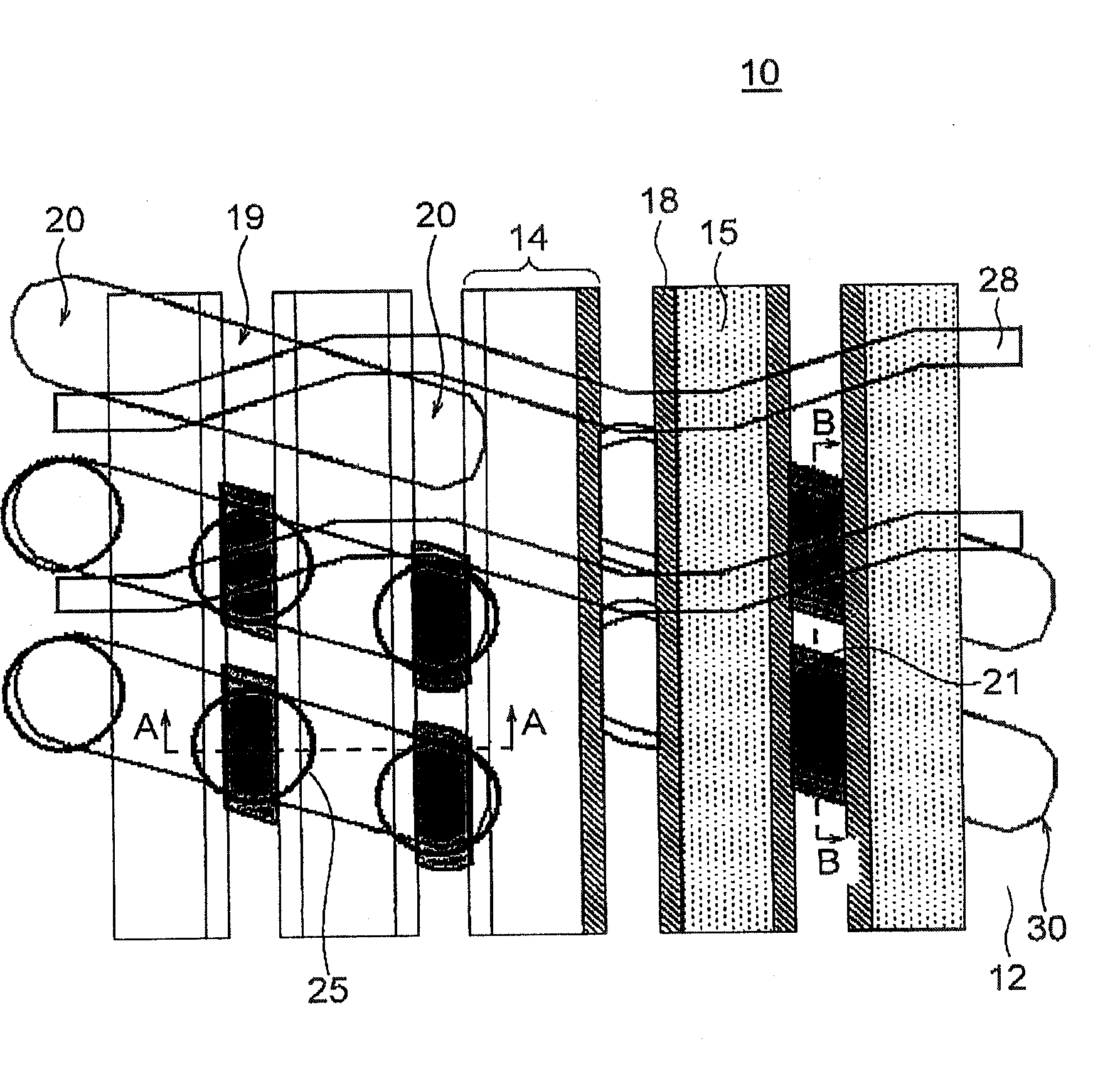
[0023]FIG. 1 is a top plan view showing the layout of a memory cell array area of a DRAM device configuring a semiconductor device according to the embodiment of the present invention. The semiconductor device 10 includes a STI structure 12 formed in the surface region of a silicon substrate for isolating the surface region thereof into a plurality of elongate device areas 30, in each of which a pair of MOSFETs are formed. A plurality of word lines, i.e., gate electrodes 15 overlie the silicon substrate while intersecting the device areas 30.

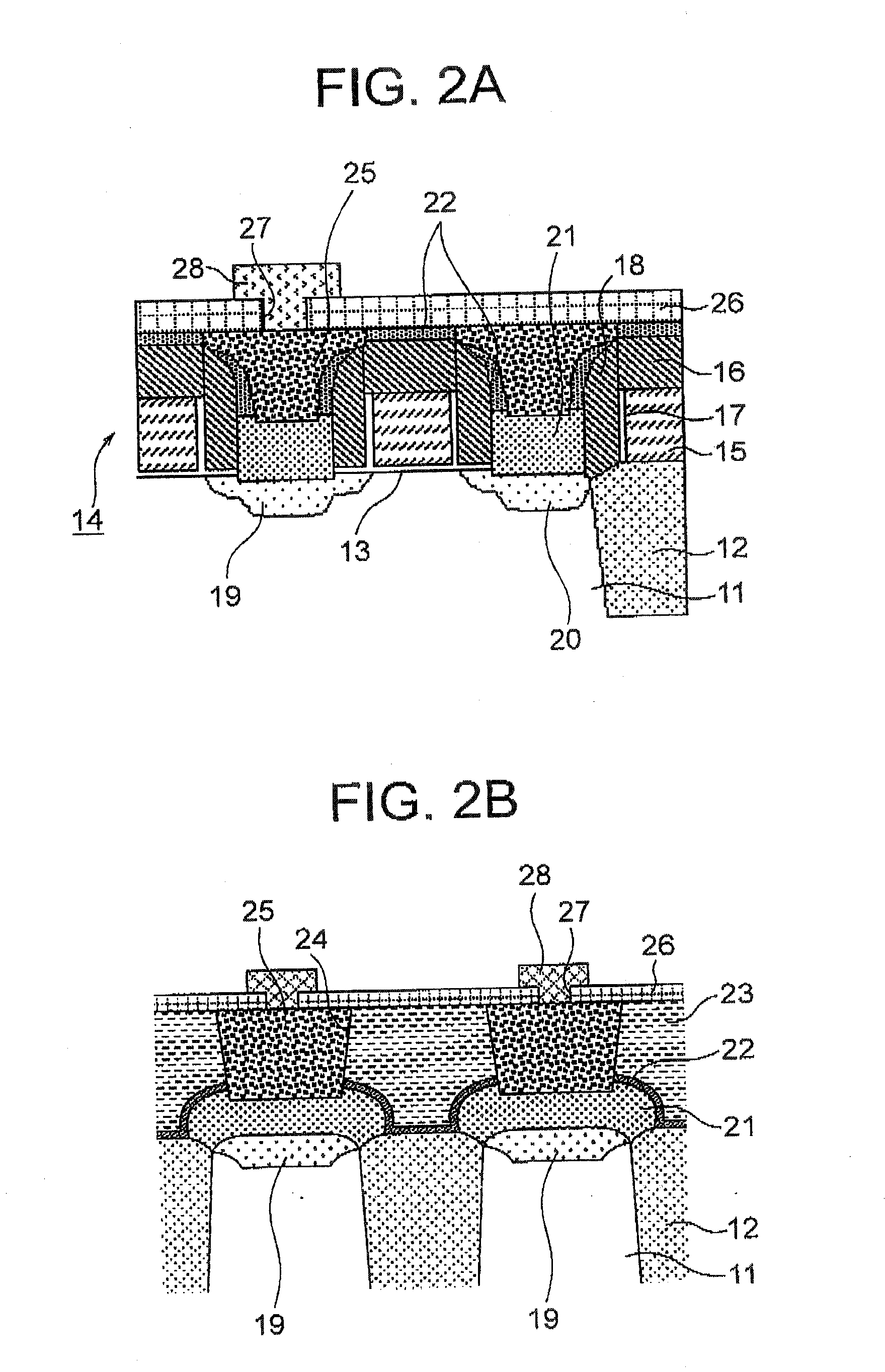
[0024]FIGS. 2A and 2B are sectional views taken along lines A-A and B-B, respectively, in FIG. 1. A gate electrode structure 14 includes the gate electrode 15 formed on a gate insulating film 13, an overlying protective film...


PUM


Abstract

A method for manufacturing a semiconductor device includes the steps of epitaxially growing silicon to form a first contact layer in a first opening exposing therethrough a portion of a silicon substrate; forming a dielectric film having a second opening exposing therethrough the top surface of the first contact layer; and epitaxially growing silicon in the second opening on the surface of the first contact layer to form a second contact layer. The first and second contact layers in combination configure a contact plug.

Description

BACKGROUND OF THE INVENTION[0001](a) Field of the Invention[0002]The present invention relates to a semiconductor device and, more particularly, to the structure of an epitaxially grown contact plug formed in the semiconductor device. The present invention also relates to a method for manufacturing such a semiconductor device.[0003](b) Description of the Related Art[0004]DRAM (dynamic random access memory) devices include an array of memory cells each configuring a storage unit for storing therein a binary data. The memory cell includes a MOSFET (metal-oxide-semiconductor field-effect-transistor) formed in the surface region of a semiconductor substrate and a capacitor connected to the MOSFET, and stores therein data by storing electric charge in the capacitor via the MOSFET. In recent years, the line space and width in the semiconductor device has drastically reduced along with the development of the higher integration and higher performance of the semiconductor device. The reducti...

Claims


Application Information

Patent Timeline
Patent Type & Authority Applications(United States)
IPC IPC(8): H01L23/52H01L21/44
CPCH01L21/28525H01L21/76879H01L21/76897H01L27/10855H01L27/10888H01L2924/0002H01L27/10894H01L2924/00H10B12/0335H10B12/485H10B12/09
Inventor TANAKA, YOSHINORI
Owner ELPIDA MEMORY INC
Why Eureka
Try Eureka