Apparatus for testing electronic devices

Active Publication Date: 2008-04-03
AEHR TEST SYST
View PDF1 Cites 24 Cited by
  • Summary
  • Abstract
  • Description
  • Claims
  • Application Information

AI Technical Summary

Benefits of technology

[0151]The method may further include delaying turning the power voltage to the

Problems solved by technology

One challenge in full wafer testing is that there are a large amount of contacts on a waf

Method used


Image

  • Apparatus for testing electronic devices
  • Apparatus for testing electronic devices
  • Apparatus for testing electronic devices

Examples


Embodiment Construction

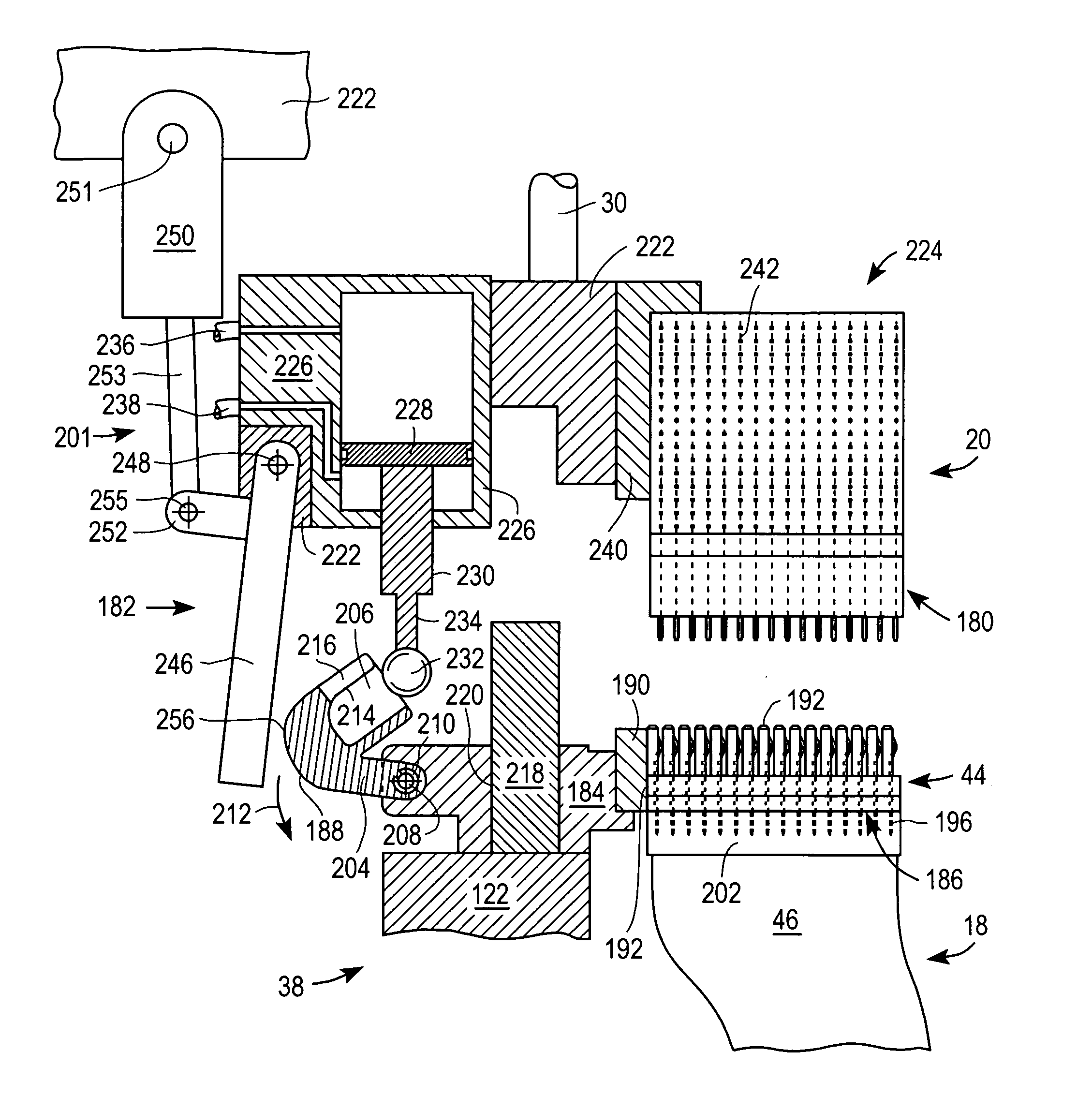
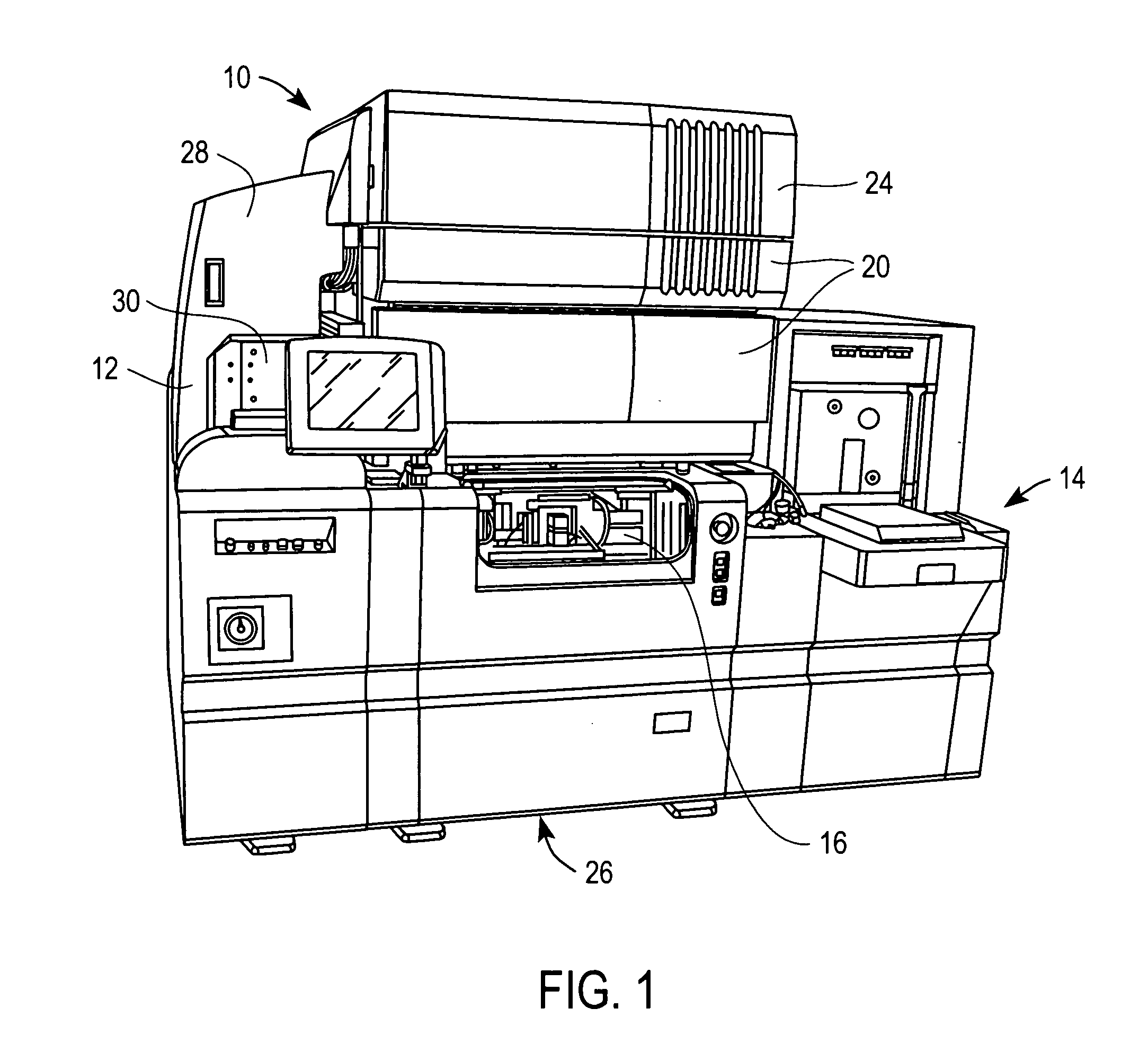
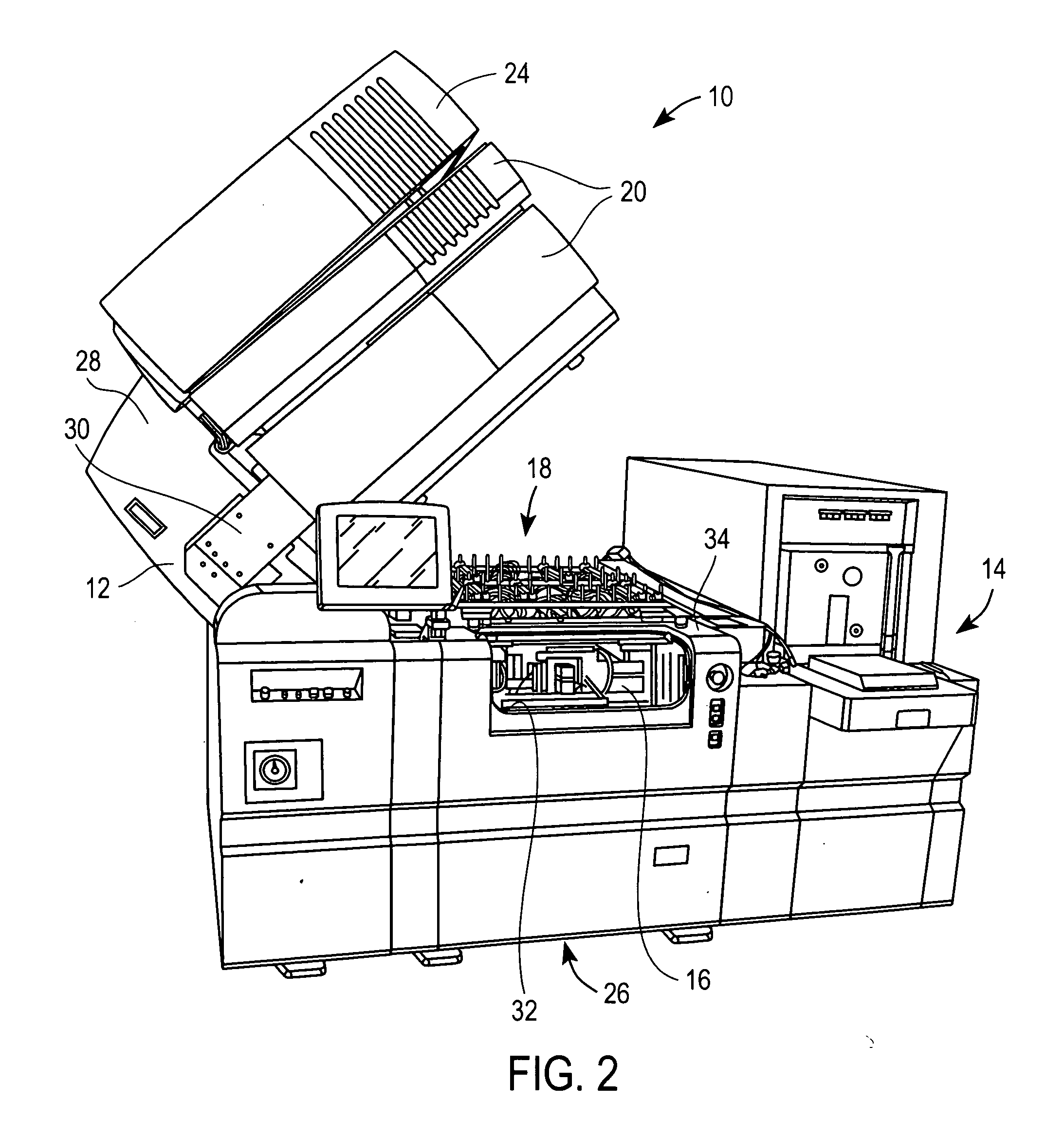
[0277]FIGS. 1 and 2 of the accompanying drawings illustrate an apparatus 10, which is particularly suitable for full-wafer testing of microelectronic circuits of unsingulated wafers and / or burn-in testing of unsingulated wafers and / or built-in self-testing of unsingulated wafers. The apparatus 10 includes a frame 12 and a number of modules mounted to the frame 12 including a wafer loader 14, a probing subassembly 16, a cartridge 18, a test head 20, and a thermal system 24.

[0278]The frame 12 has a prober base portion 26, a thermal system frame portion 28, and a test head frame portion 30. The thermal system frame portion 28 is pivotally mounted to the prober base portion 26. The test head frame portion 30 is pivotally mounted to the thermal system frame portion 28. The probing subassembly 16 and the cartridge 18 are mounted to lower and upper portions 32 and 34 respectively of the prober base portion 26, the test head 20 and the thermal system 24 are mounted to the test head frame po...


PUM


Abstract

The invention provides an apparatus for testing an integrated circuits on devices including a plurality of electrical subassemblies including a plurality of pattern generator, driver, and power boards divided into physical zones with each physical zone including one pattern generator board, at least one driver board, and at least one power board connected to one another; and a configuration file having information representing flow of current through the electrical subassemblies connected to one another in an interconnection scheme, wherein the electrical subassemblies are organized into at least one logical zone, and wherein the logical zone comprises a plurality of pattern generators.

Description

BACKGROUND OF THE INVENTION[0001]1). Field of the Invention[0002]This invention relates to an apparatus that is used for full-wafer testing and / or burn-in testing and / or built-in self-testing.[0003]2). Discussion of Related Art[0004]Microelectronic circuits are usually fabricated in and on semiconductor wafers. Such a wafer is subsequently “singulated” or “diced” into individual dies. Such a die is typically mounted to a supporting substrate for purposes of providing rigidity thereto and electronic communication with an integrated or microelectronic circuit of the die. Final packaging may include encapsulation of the die and the resulting package can then be shipped to a customer.[0005]It is required that the die or the package be tested before being shipped to a customer. Ideally, the die should be tested at an early stage for the purposes of identifying the defects that occur during early stage manufacturing.[0006]The earliest stage that a die can be tested is after completion of ...

Claims


Application Information

Patent Timeline
IPC IPC(8): G01R31/02
CPCG01R31/2877G01R31/2891G01R31/31926G01R31/31908G01R31/31905
Inventor MAENNER, THOMAS T.
Owner AEHR TEST SYST
Why Eureka
Try Eureka