Integrated magnetic features

a magnetic feature and integrated technology, applied in the direction of magnetic bodies, transformers/inductance details, electromagnets with armatures, etc., can solve the problems of inconvenient use of conventional methods for forming such structures, and the inability to form micron to nanometer-scale magnetic components or directly into semiconductor-based integrated circuit devices

Inactive Publication Date: 2008-04-03
APPLIED MATERIALS INC
View PDF16 Cites 64 Cited by
  • Summary
  • Abstract
  • Description
  • Claims
  • Application Information

AI Technical Summary

Problems solved by technology

Current conventional methods used to form such structures are poorly suited to form micron to nanometer scale magnetic components or for incorporating them directly into semiconductor based integrated circuit devices.

Method used


Image

  • Integrated magnetic features
  • Integrated magnetic features
  • Integrated magnetic features

Examples


Embodiment Construction

[0024]The present invention generally relates to the process of forming an magnetic device that may be used to form a component contained within a micro-mechanical or nano-magnetic device, such as a pressure or position sensor, a voice coil, an accelerometer, a micro-mirror, or an optical switch, using various semiconductor processing techniques. Embodiment of the invention may further provide an apparatus and method of orienting and / or physically aligning a substrate to an external reference having a similar orientation of magnetic device elements.

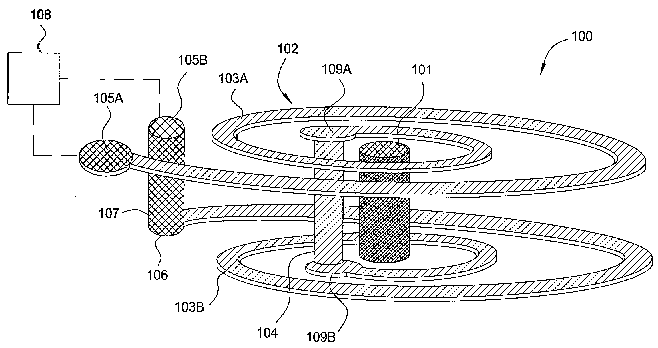
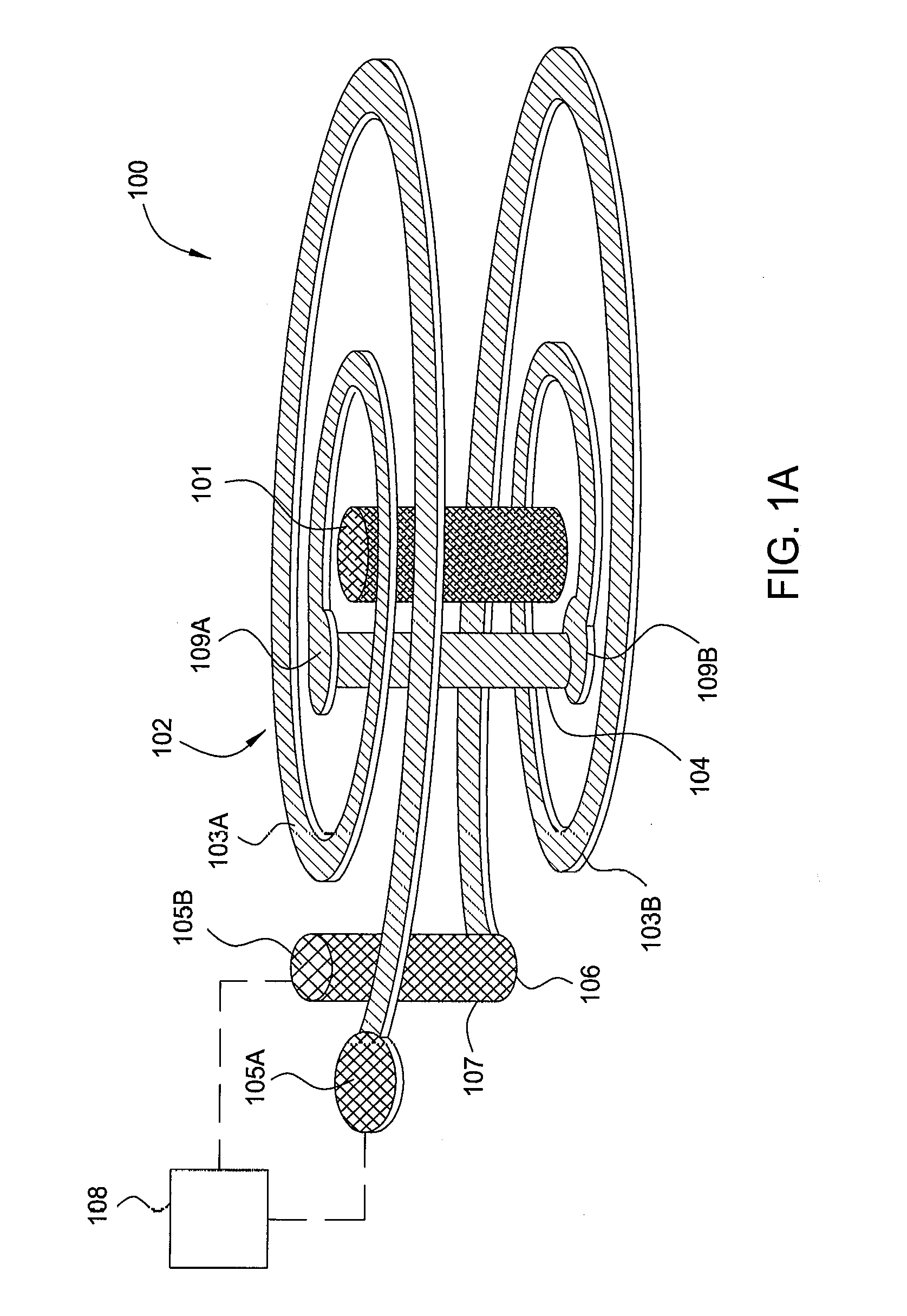
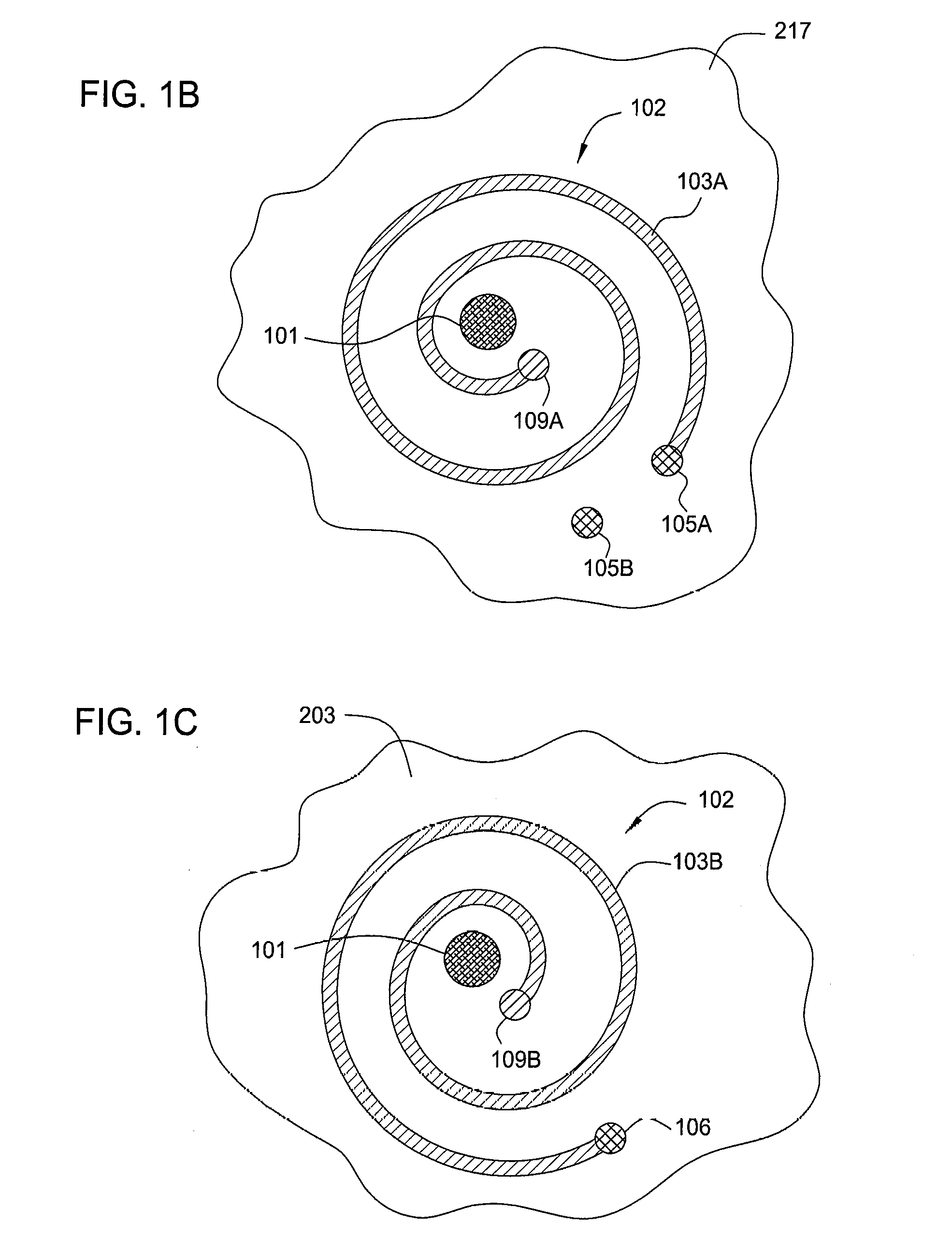
[0025]FIG. 1A is an isometric view of one embodiment in which an electromagnet device 100 is formed using a dual damascene type process. The various process steps used to form the electromagnet device 100 are illustrated in FIG. 2 and FIGS. 3A-3I. The electromagnet device 100 generally contains a core 101 and a coil 102 that are formed in a portion of the substrate (e.g., substrate 201 in FIGS. 3A-3I). One will note that the dielectric la...


PUM

PropertyMeasurementUnit
temperatureaaaaaaaaaa
thickaaaaaaaaaa

Abstract

The present invention generally relates to the process of forming a magnetic element or magnetic device that may be used to form a component within an integrated circuit device using a combination of electroless plating and various standard semiconductor processing techniques. In one embodiment, a plurality of magnetic devices are formed on a surface of a substrate so that the orientation of features on the surface of the substrate can be ascertained. In one embodiment, the magnetic devices formed on a surface of a substrate are used to physically align a substrate to an external reference having a similar orientation of magnetic elements.

Description

BACKGROUND OF THE INVENTION[0001]1. Field of the Invention[0002]Embodiments of the present invention generally relate to micromechanical or nano-mechanical devices that require electromagnetic components, and methods of forming the same.[0003]2. Description of the Related Art[0004]Micro-mechanical or nanomechanical magnetic type devices that utilize magnetic materials and coil shaped structures have been discussed in the art, such as a device described in the United State Publication Patent Application No. 20040244488. Common micro-mechanical or nanomechanical devices may be voice coils, electromagnets, sensors (e.g., accelerometers), inductors, or other similar devices. One common component found in these micro-mechanical or nanomechanical devices are magnetic components that are formed on a substrate to provide some driving force to cause some useful motion, detect either motion or position of a component relative to some external reference, and / or allow some information or data t...

Claims


Application Information

Patent Timeline
Patent Type & Authority Applications(United States)
IPC IPC(8): H01F27/28
CPCH01F5/003H01F2007/068H01F7/08
Inventor WEIDMAN, TIMOTHY W.
Owner APPLIED MATERIALS INC
Why Eureka
Try Eureka