Pixel structure

a liquid crystal display and structure technology, applied in non-linear optics, instruments, optics, etc., can solve the problems of reducing cell gap, reducing color washout, and reducing cell gap, so as to reduce color washout, maintain yield and brightness, and solve mura and residual image problems

Active Publication Date: 2008-04-03
AU OPTRONICS CORP
View PDF5 Cites 13 Cited by
  • Summary
  • Abstract
  • Description
  • Claims
  • Application Information

AI Technical Summary

Benefits of technology

[0008]Accordingly, the present invention is directed to provide a pixel structure for reducing color washout, maintaining yield and brightness, and resolving mura and residual image problems.
[0025]With the use of the foregoing structure in the present invention, the first pixel electrode, the second pixel electrode and the third pixel electrode all have different voltage values when the pixel structure is driven. Hence, the liquid crystal molecules on the pixel structure can have various tilt angles to reduce the color washout problem.

Problems solved by technology

Although a thin film transistor liquid crystal display with multi-domain vertical alignment can achieve the purpose of having a wide viewing angle, the presence of color washout problem is a major drawback.
However, the effect produced by using a retardation film is quite limited, and reducing the cell gap would lower the yield and brightness.
On the other hand, the method of forming two different liquid crystal capacitors of a single pixel structure requires the formation of an additional dielectric layer, which may cause mura and residual image problems.

Method used


Image

  • Pixel structure
  • Pixel structure
  • Pixel structure

Examples


first embodiment

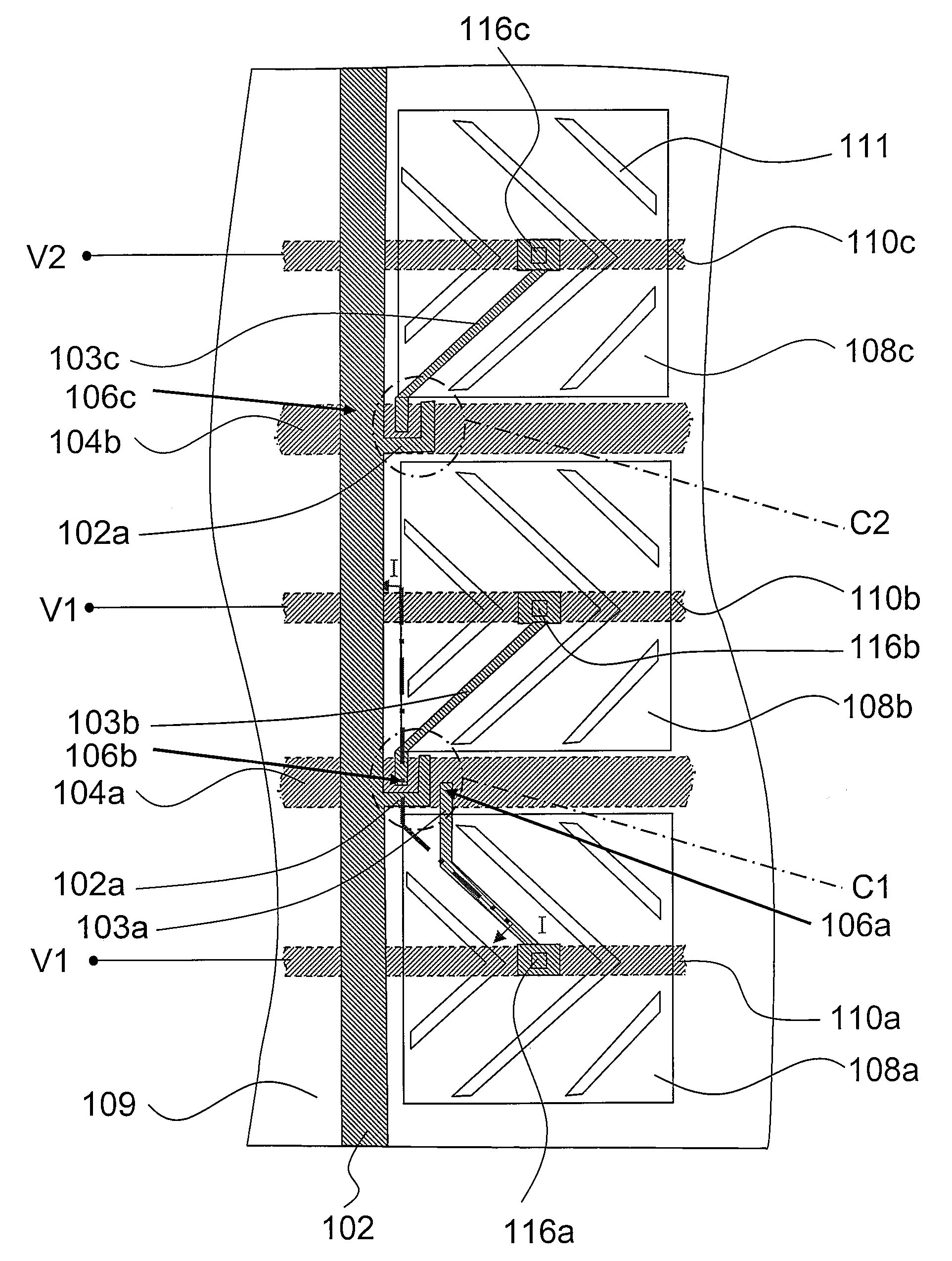
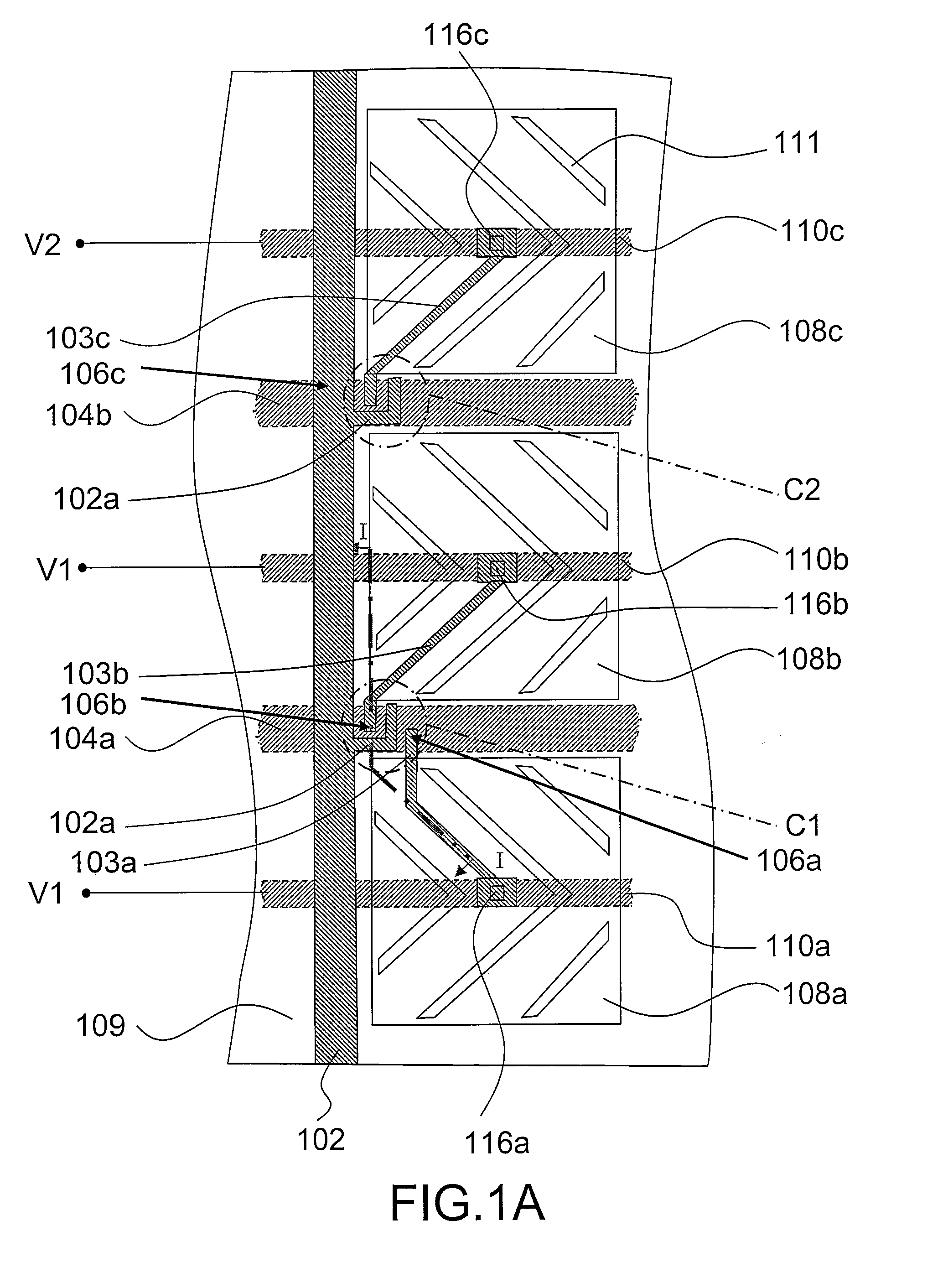
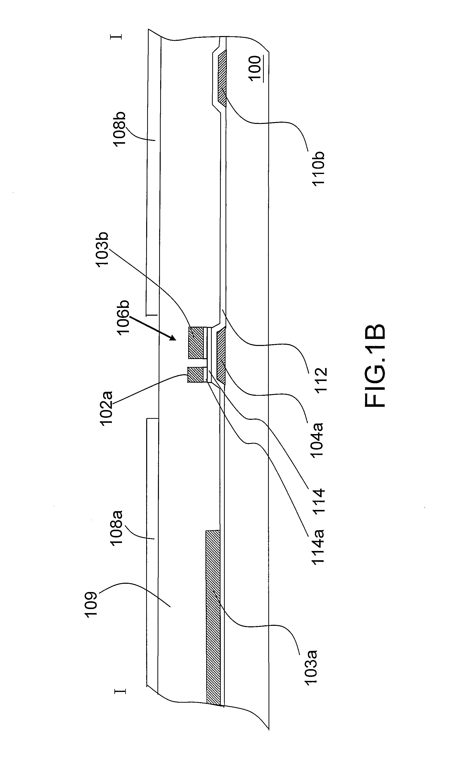
[0038]FIG. 1A is a top view of a pixel structure according to a first embodiment of the present invention. FIG. 1B is a schematic view along cross-sectional line I-I of FIG. 1A. FIG. 1C is a locally magnified view of area C1 in FIG. 1A. FIG. 1D is a locally magnified view of area C2 in FIG. 1A.

[0039]As shown in FIGS. 1A and 1B, the pixel structure in the present embodiment comprises a substrate 100, a data line 102, a first scan line 104a, a second scan line 104b, a first thin film transistor 106a, a second thin film transistor 106b, a third thin film transistor 106c, a first pixel electrode 108a, a second pixel electrode 108b, a third pixel electrode 108c, a first common line 110a, a second common line 110b and a third common line 110c. The data line 102, the first scan line 104a and the second scan line 104b are disposed over the substrate 100. The first thin film transistor 106a, the second thin film transistor 106b and the third thin film transistor 106c are electrically connect...

second embodiment

[0051]FIG. 3A is a top view of a pixel structure according to a second embodiment of the present invention. FIG. 3B is a schematic view along cross-sectional line II-II of FIG. 3A. In the second embodiment, the components of the pixel structure identical to the ones in the first embodiment are labeled identically. Moreover, only the portions that are different from the first embodiment are described below. In addition, any types of extensions that are applicable to the first embodiment may also be applied to the pixel structure of the second embodiment.

[0052]As shown in FIGS. 3A and 3B, the main difference between the pixel structure in the second embodiment and the one in the first embodiment is that the first width-to-length ratio W1 / L1, the second width-to-length ratio W2 / L2 and the third width-to-length ratio W3 / L3 are all the same. Similarly, the first common line 110a and the second common line 110b are electrically connected to the first voltage V1 and the third common line 1...


PUM

PropertyMeasurementUnit
width-to-length ratioaaaaaaaaaa
voltageaaaaaaaaaa
impedanceaaaaaaaaaa

Abstract

A pixel structure is provided. A scan line and a data line are disposed over a substrate. A first, second, and third thin film transistors are electrically connected with the data line and the scan line. The width-to-length ratios of the second and third thin film transistors are the same but larger than that of the first thin film transistor. A first, second and third pixel electrodes are electrically connected with the first, the second and the third thin film transistors, respectively. A first, second and third common lines are disposed below the first, second and third pixel electrodes respectively. The first and second common lines are electrically connected to a first voltage and the third common line is electrically connected to a second voltage.

Description

CROSS-REFERENCE TO RELATED APPLICATION[0001]This application claims the priority benefit of Taiwan application serial no. 95136208, filed Sep. 29, 2006. All disclosure of the Taiwan application is incorporated herein by reference.BACKGROUND OF THE INVENTION[0002]1. Field of the Invention[0003]The present invention relates to a pixel structure, and more particularly to a pixel structure of a liquid crystal display.[0004]2. Description of Related Art[0005]Because of the high picture quality, high spatial utilization, low power consumption, radiation-free operation of thin film transistor liquid crystal display (TFT-LCD), it has become one of the mainstream displays in the market. At present, some of the basic demands on the liquid crystal display include properties such as a high contrast ratio, rapid response and wide viewing angle. The technologies capable of providing a wide viewing angle include, for example, multi-domain vertical alignment (MVA), multi-domain horizontal alignment...

Claims


Application Information

Patent Timeline
Patent Type & Authority Applications(United States)
IPC IPC(8): G02F1/1343
CPCG02F1/136286G02F1/134309
Inventor CHIU, CHUN-CHANGCHU, SHIH-CHANGYANG, CHIH-MIN
Owner AU OPTRONICS CORP
Why Eureka
Try Eureka