Thermography measurement system for conducting thermal characterization of integrated circuits

a technology of thermal characterization and integrated circuit, which is applied in the direction of electrical/magnetic measurement arrangements, amplifier modifications to reduce noise influence, compasses, etc., can solve the problems of reducing performance and reliability, understanding and determining the thermal behavior of modern electronics, and computational approaches can provide, so as to achieve accurate and efficient thermal characterization of fully three-dimensional active micro-devices, fast and accurate resolution of geometric and material complexity, the effect of high spatial and temporal accuracy

Active Publication Date: 2008-04-03
RAAD PETER E
View PDF5 Cites 38 Cited by
  • Summary
  • Abstract
  • Description
  • Claims
  • Application Information

AI Technical Summary

Benefits of technology

[0011]The present invention overcomes most of the disadvantages and problems associated with thermal characterization of submicron semiconductor devices. It combines a system capable of mapping the surface temperature of a complex device with high spatial and temporal accuracy, a computational engine capable of rapidly and accurately resolving the geometric and material complexities of a full three-dim

Problems solved by technology

As semiconductor devices become physically more complex with shrinking feature sizes and higher local power densities, cooling problems multiply, which can lead to a decrease in performance and reliability.
Thus, understanding and determining the thermal behavior of modern electronics has become a key issue in their design.
Computational approaches can provide insight into the internal thermal behavior of such complex devices, but can be limited by the inherent necessity of modeling the heat sources, which in the case of self-heating microelectronic devices, are the result of electrical fields whose exact shapes and locations are difficul

Method used


Image

  • Thermography measurement system for conducting thermal characterization of integrated circuits
  • Thermography measurement system for conducting thermal characterization of integrated circuits
  • Thermography measurement system for conducting thermal characterization of integrated circuits

Examples


Embodiment Construction

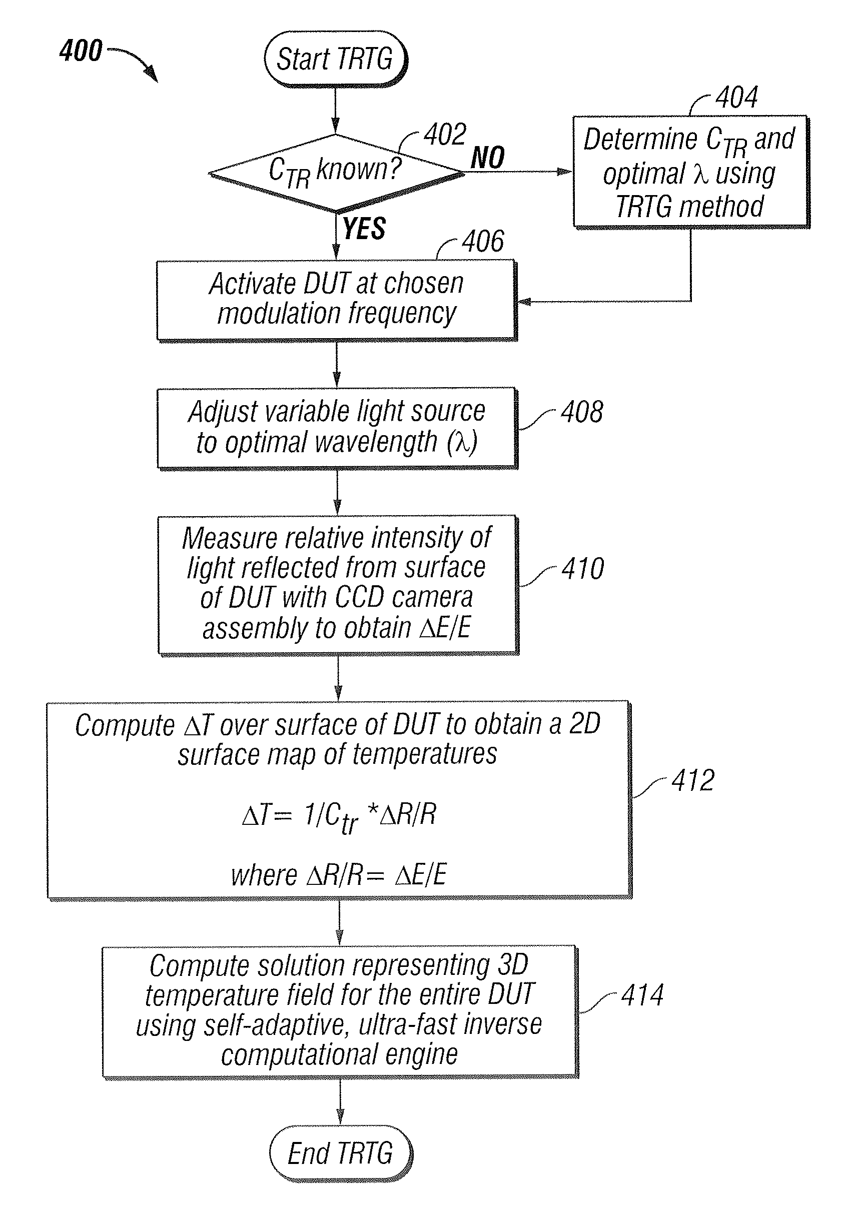
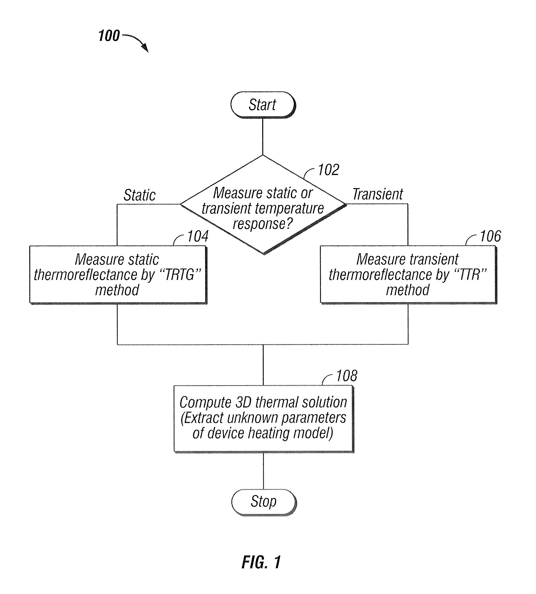
[0031]FIG. 1 represents the high-level flow diagram of the basic operation of the present invention as it is used to measure the three-dimensional temperature field distribution of an active semiconductor micro-device. To conduct a full three-dimensional temperature characterization of a device requires essentially three steps 100. First, because different equipment is required, a decision must be made as to whether the static or transient thermal distribution is sought 102. Second, a two-dimensional thermal measurement is conducted. If static data is required, then CCD camera-based Thermoreflectance Thermography system (TRTG) is used 104. If transient data is required, then a laser-based TRTG is used 106. Third, a three-dimensional thermal characterization is computed from the two-dimensional data and various device parameters 108.

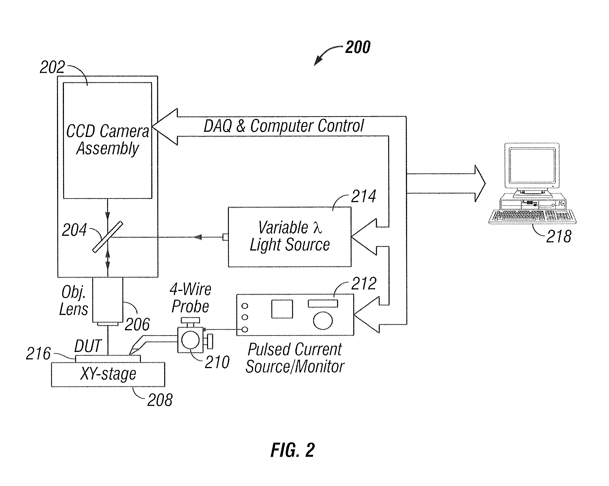
[0032]The present invention is based on the thermoreflectance (TR) method, where the change in surface temperature is measured by detecting the change in...


PUM


Abstract

A system and method to fully characterize the thermal behavior of complex 3D submicron electronic devices. The system replaces and/or supplements laser-based surface temperature scanning with a CCD camera-based approach. A CCD camera records multiple points of light energy reflected from an integrated circuit to obtain a static temperature measurement. The system is used to non-invasively measure with submicron resolution the 2D surface temperature field of an activated device. A CW laser illuminates a single point on the surface of an active device and a photodetector records the reflected light energy to obtain a transient temperature measurement. The measured 2D temperature field is used as input for an ultra-fast inverse computational solution to fully characterize the thermal behavior of the complex 3D device. The system extracts geometric features of a known device, assessing the system's ability to combine measured results and computations to fully characterize complex 3D electronic devices.

Description

CROSS-REFERENCES TO RELATED APPLICATIONS[0001]Not ApplicableSTATEMENT REGARDING FEDERALLY SPONSORED RESEARCH OR DEVELOPMENT[0002]Not ApplicableTHE NAMES OF THE PARTIES TO A JOINT RESEARCH AGREEMENT[0003]Not ApplicableINCORPORATION-BY-REFERENCE OF MATERIAL SUBMITTED ON A COMPACT DISC[0004]Not ApplicableBACKGROUND OF THE INVENTION[0005]1. Field of the Invention[0006]The present invention relates generally to semiconductor thermography and more specifically to a system and method for measuring the thermal behavior of integrated circuits.[0007]2. Description of Related Art[0008]The present invention references Applicant's U.S. Pat. No. 6,064,810, the contents of which are incorporated herein by reference.[0009]As semiconductor devices become physically more complex with shrinking feature sizes and higher local power densities, cooling problems multiply, which can lead to a decrease in performance and reliability. Thus, understanding and determining the thermal behavior of modern electro...

Claims


Application Information

Patent Timeline
IPC IPC(8): G06F19/00
CPCG01K11/125
Inventor RAAD, PETER E.
Owner RAAD PETER E
Why Eureka
Try Eureka