Mosfet with body contacts

a technology of mosfet and body, applied in the direction of mosfet devices, basic electric elements, electrical appliances, etc., can solve the problems of threshold voltage shifting within the semiconductor device, and the device fabricated within the semiconductor-on-insulator substrate is not entirely without difficulties

Inactive Publication Date: 2008-04-10
IBM CORP
View PDF4 Cites 128 Cited by
  • Summary
  • Abstract
  • Description
  • Claims
  • Application Information

AI Technical Summary

Benefits of technology

[0011]The invention includes a semiconductor structure and a method for fabricating the semiconductor structure. The semiconductor structure and the method for fabricating the semiconductor structure include use of a body contact region. The body contact region is recessed with respect to a surface of a channel region located over a body region within the semiconductor structure to avoid electrical shorting between the body contact region and source / drain regions (in particular source / drain region extensions) within the semiconductor structure.

Problems solved by technology

Although semiconductor-on-insulator substrates are thus often essential in semiconductor device fabrication to provide enhanced performance semiconductor devices, devices fabricated within semiconductor-on-insulator substrates are nonetheless not entirely without difficulties.
A floating body effect within a semiconductor device often causes for a threshold voltage shifting within the semiconductor device.

Method used


Image

  • Mosfet with body contacts
  • Mosfet with body contacts
  • Mosfet with body contacts

Examples


Embodiment Construction

[0017]The invention, which includes a semiconductor structure and a method for fabricating the semiconductor structure, is understood within the context of the description provided below. The description provided below is understood within the context of the drawings described above. Since the drawings are intended for illustrative purposes, the drawings are not necessarily drawn to scale.

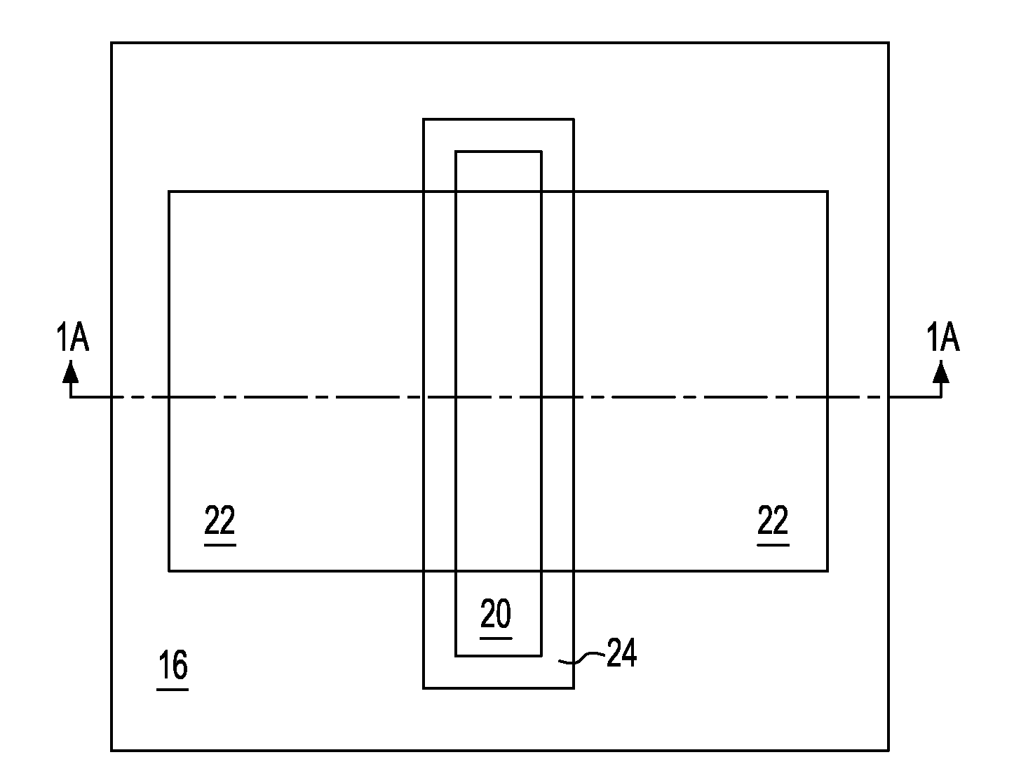
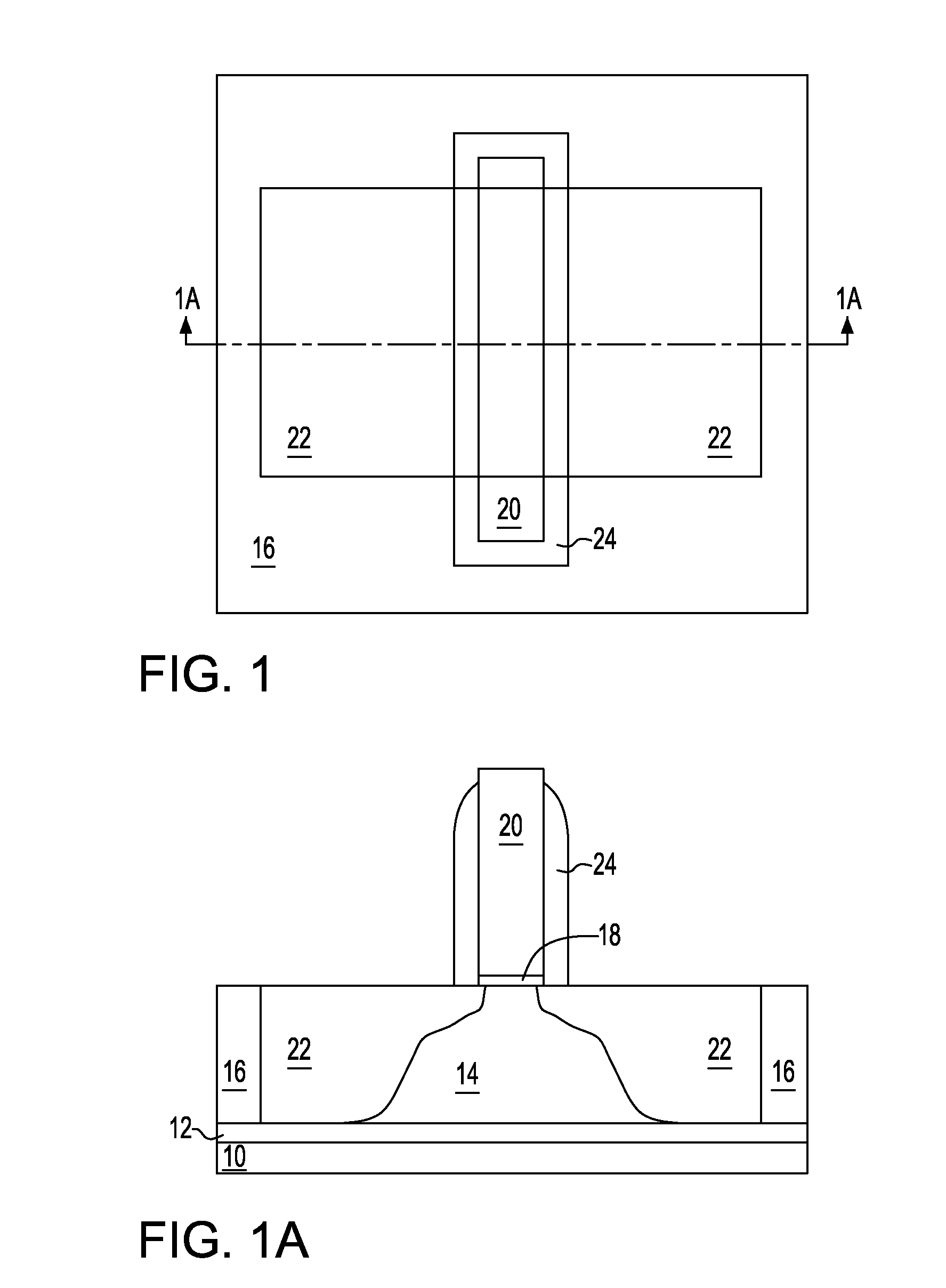
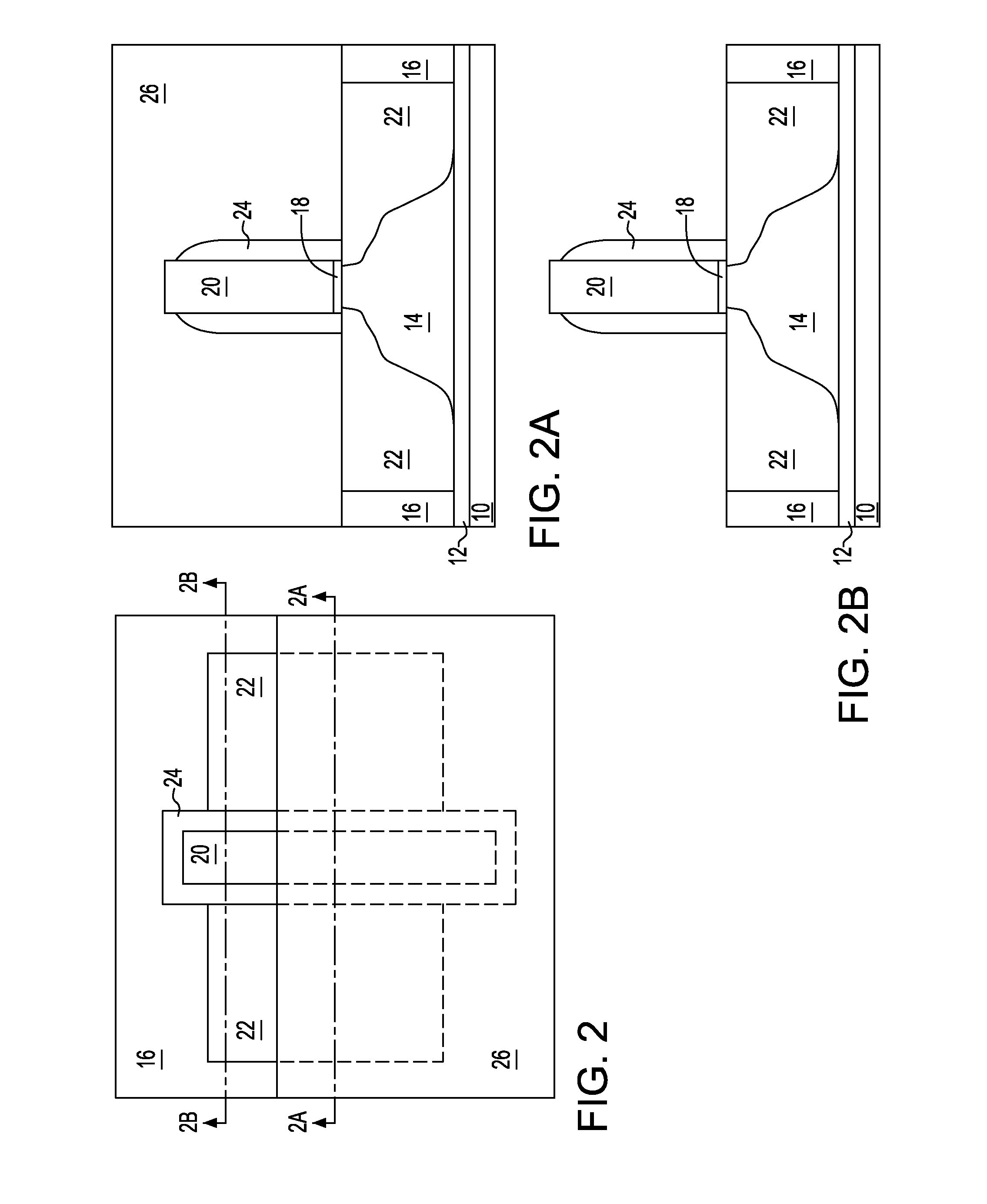
[0018]FIG. 1 to FIG. 7C show a series of schematic plan-view and cross-sectional diagrams illustrating the results of progressive stages in fabricating a semiconductor structure in accordance with an embodiment of the invention. This particular embodiment of the invention comprises a preferred embodiment of the invention. FIG. 1 shows a schematic plan-view diagram, and FIG. 1A shows a schematic cross-sectional diagram, of the semiconductor structure at an early stage in the fabrication thereof in accordance with the preferred embodiment.

[0019]FIG. 1A in particular shows a base semiconductor substra...


PUM


Abstract

A semiconductor structure includes a metal oxide semiconductor field effect transistor that includes a body contact region that extends from body region located beneath a channel region that separates a pair of source / drain regions within the metal oxide semiconductor field effect transistor. The body contact region is recessed with respect to a surface of the channel region to avoid shorting between a body contact and the source / drain regions.

Description

BACKGROUND[0001]1. Field of the Invention[0002]The invention relates generally to semiconductor structures. More particularly, the invention relates to semiconductor structures with enhanced performance and reliability.[0003]2. Description of the Related Art[0004]Recent advances in semiconductor technology have included the use of semiconductor-on-insulator substrates when fabricating semiconductor devices. Semiconductor-on-insulator substrates are desirable insofar as semiconductor-on-insulator substrates provide for superior semiconductor device isolation, and also for uniformly thinner channel regions within semiconductor devices.[0005]Although semiconductor-on-insulator substrates are thus often essential in semiconductor device fabrication to provide enhanced performance semiconductor devices, devices fabricated within semiconductor-on-insulator substrates are nonetheless not entirely without difficulties. In particular, due to the superior isolation capabilities of semiconduct...

Claims


Application Information

Patent Timeline
Patent Type & Authority Applications(United States)
IPC IPC(8): H01L27/12
CPCH01L29/78615
Inventor ZHU, HUILONGLUO, ZHIJIONG
Owner IBM CORP
Why Eureka
Try Eureka