
Optical semiconductor device

a technology of optical semiconductors and semiconductors, applied in the direction of optical waveguide light guides, instruments, optics, etc., can solve the problems of disadvantageous increase in optical waveguide loss, and achieve the effect of reducing waveguide loss at the bent portion of optical waveguide, and increasing waveguide light efficiency

Active Publication Date: 2008-04-10
SONY CORP
View PDF3 Cites 39 Cited by
  • Summary
  • Abstract
  • Description
  • Claims
  • Application Information

AI Technical Summary

Benefits of technology

[0010]Accordingly, it is desirable to decrease the optical waveguide loss at a bent portion of an optical waveguide.
[0012]In the optical semiconductor device described above, since at least one insulating film region is formed in the semiconductor region and above at least one of the outside and the inside with respect to the central part of the bent portion of the optical waveguide, the waveguide loss at the bent portion of the optical waveguide is decreased. The reason for this is believed that the insulating film region enables light which is guided in the optical waveguide and which is to be emitted outside at the bent portion of the optical waveguide to return to the inside thereof.
[0013]According to the optical semiconductor device of the embodiment of the present invention, since the waveguide loss at the bent portion of the optical waveguide can be decreased, the waveguide efficiency of light can be increased, and as a result, an optical semiconductor device having a high-performance optical waveguide can be advantageously provided.

Problems solved by technology

The problem to be solved by the present invention is that since a ridge-type optical waveguide generally has not strong light confinement, when it is compared with a strip-type optical waveguide, an optical waveguide loss is disadvantageously increased when the optical waveguide is bent.

Method used


Image

  • Optical semiconductor device
  • Optical semiconductor device
  • Optical semiconductor device

Examples


Embodiment Construction

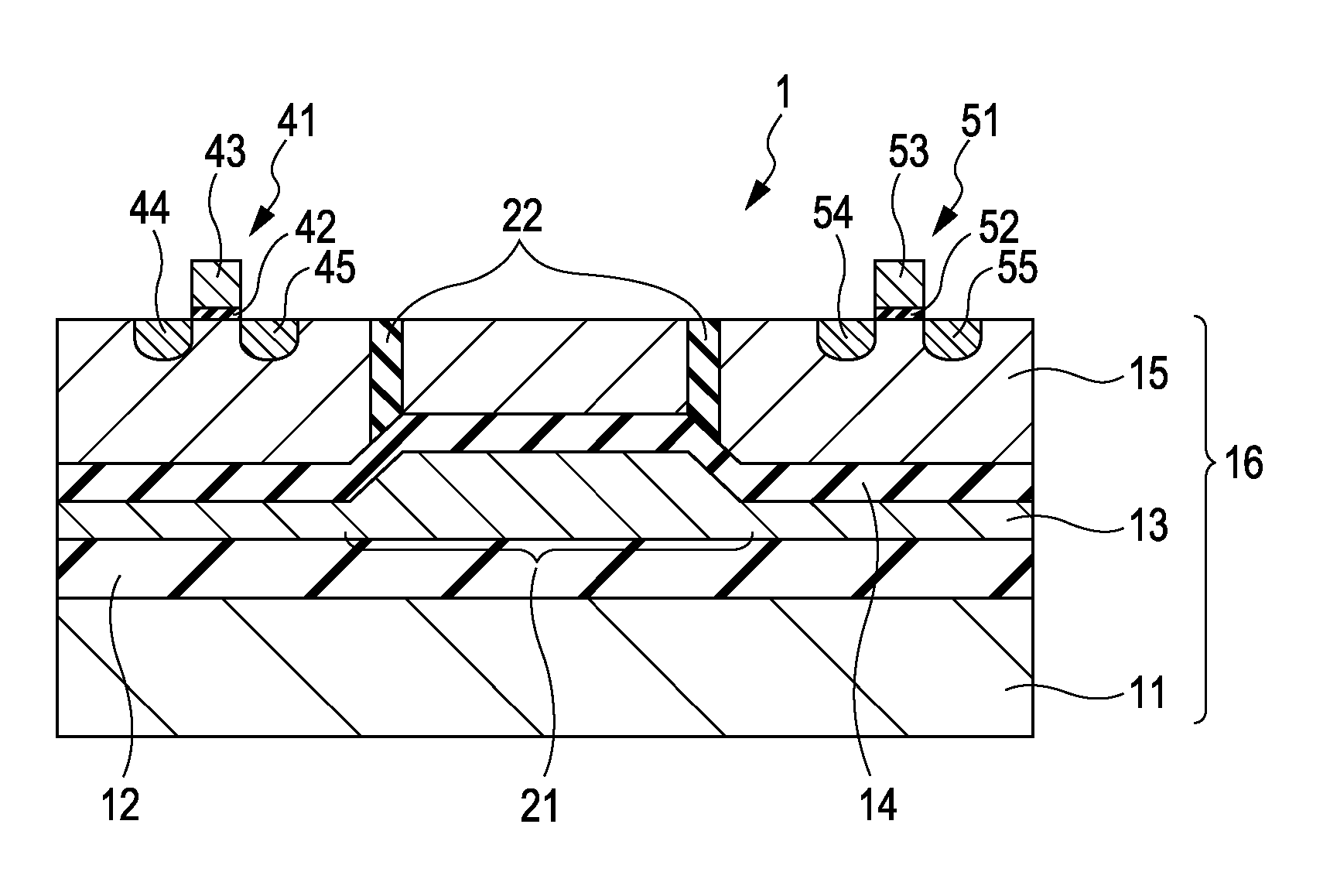
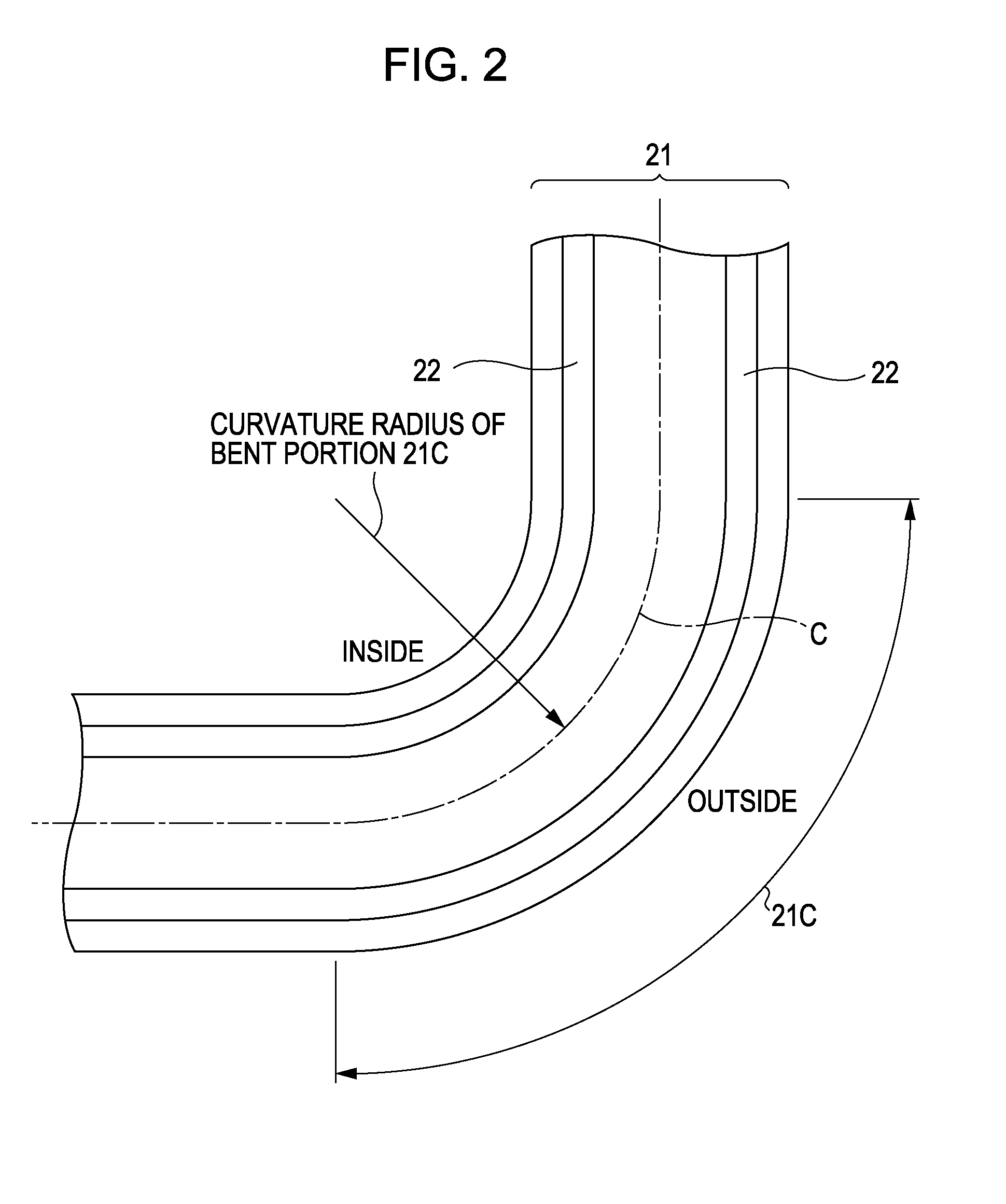
[0027]An optical semiconductor device 1 according to one embodiment (first example) of the present invention will be described with reference to a schematic cross-sectional structural view of FIG. 1 and a plan layout view of FIG. 2.

[0028]As shown in FIG. 1, there are provided a semiconductor substrate 11, a first semiconductor layer 13 which is formed on the semiconductor substrate 11 with a first light confinement layer 12 interposed therebetween so that a region to be used as an optical waveguide 21 has a thickness larger than that of the other region, and a second semiconductor layer 15 formed on the first semiconductor layer 13 with a second light confinement layer 14 interposed therebetween. As the semiconductor substrate 11, for example, a silicon substrate is used. In addition, the first light confinement layer 12 and the second light confinement layer 14 are formed of an insulating film having a refractive index lower than that of the semiconductor layer described above and ...


PUM


Abstract

Since a ridge-type optical waveguide generally has not strong light confinement, when it is compared with a strip-type optical waveguide, an optical waveguide loss is increased when the optical waveguide is bent. Accordingly, it is desirable to decrease an optical waveguide loss at a bent potion of the waveguide. An optical waveguide is provided which includes a semiconductor region, an optical waveguide provided between a first light confinement layer and a second light confinement layer formed in the semiconductor region, and at least one insulating film region formed in the semiconductor region and above at least one of an outside and an inside with respect to a curvature radius direction of the bent portion of the optical waveguide.

Description

CROSS REFERENCES TO RELATED APPLICATIONS[0001]The present invention contains subject matter related to Japanese Patent Application JP 2006-274752 filed in the Japanese Patent Office on Oct. 6, 2006, the entire contents of which are incorporated herein by reference.BACKGROUND OF THE INVENTION[0002]1. Field of the Invention[0003]The present invention relates to an optical semiconductor device having an optical waveguide which decreases a waveguide loss at a bent portion thereof.[0004]2. Description of the Related Art[0005]There has been a method for forming an optical waveguide immediately under the surface of a silicon substrate by a SIMOX (Separation by Implanted Oxygen) method. This method is characterized in that a portion to be used as an optical waveguide can be formed inside a single crystalline silicon material while the surface thereof is allowed to remain in a flat state (for example, see Prakash Koonath, Koichiro Kisima, Tejaswi Indukuri, and Bahram Jalali “Sculpting of thr...

Claims


Application Information

Patent Timeline
Patent Type & Authority Applications(United States)
IPC IPC(8): G02B6/12
CPCG02B6/122G02F1/025G02B6/125
Inventor KISHIMA, KOICHIRO
Owner SONY CORP
Features
  • Generate Ideas
  • Intellectual Property
  • Life Sciences
  • Materials
  • Tech Scout
  • Unparalleled Data Quality
  • Higher Quality Content
  • 60% Fewer Hallucinations
Learn More