Micro-pixelated fluid-assay structure with on-board addressable, pixel-specific functionalization

Inactive Publication Date: 2008-04-10
SHARP KK
View PDF20 Cites 3 Cited by
  • Summary
  • Abstract
  • Description
  • Claims
  • Application Information

AI Technical Summary

Benefits of technology

[0009]Preferably further, and in the above context, the invention takes the form of a relatively inexpensive, consumer-level-affordable DNA assay structure which features a low-cost substrate that will readily accommodate low-cost, and preferably “low-temperature-condition”, fabrication thereon of substrate-supported DNA matrix-pixel “components”. “Low temperature” is defined herein as a being a characteristic of processing that can be done on substrate material having a transition temperature (Tg) which is less than about 850° C., i.e., less than a temperature which, if maintained during sustained material processing, would cause the subject material to lose dimensional stability.
[0010]Accordingly, while the DNA matrix-pixel technology of this invention, if so desired, can be implemented on more costly supporting silicon substrates, the preferred supporting substrate material is one made of lower-expense glass or plastic materials. The terms “glass” and “p

Problems solved by technology

This imaging and template-based image-analyzing is quite time-consuming, expensive, and prone to inaccuracy.
For many reasons which are well known to those generally skilled in the relevant art, conventional micro-assay DNA probe structures are typically single-use in nature, are complex and very costly to manufacture, and are, on balance, and as was just suggested above, ultimately quite expensive to use.
These today-conventional, chip-like micro-array structures, additionally, are often frustratingly inaccurate in performance because of many false-positive responses produced during assays.
Further, assays performed with

Method used


Image

  • Micro-pixelated fluid-assay structure with on-board addressable, pixel-specific functionalization
  • Micro-pixelated fluid-assay structure with on-board addressable, pixel-specific functionalization
  • Micro-pixelated fluid-assay structure with on-board addressable, pixel-specific functionalization

Examples


Embodiment Construction

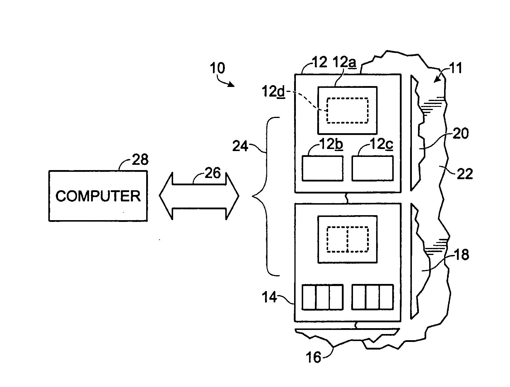
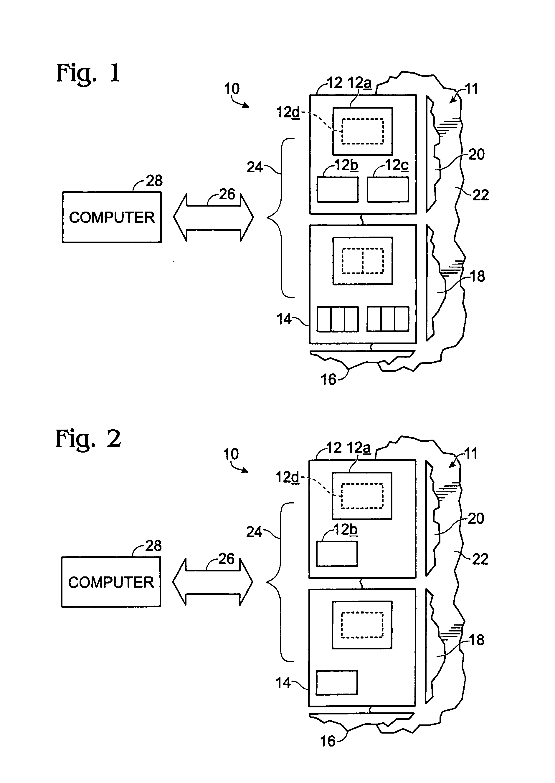
[0025]Turning now to the drawings, and referring first of all to FIG. 1, indicated generally at 10 is a fragmentary portion of a digitally-addressable, thin-film-based, pixelated, fluid-assay, active-matrix micro-structure which takes the form herein of a column-and-row array 11 of plural, individually addressable micro-pixels, or pixels, such as those shown at 12, 14, 16, 18, 20, formed, as will shortly be described (but generally utilizing low-temperature TFT and Si technology as mentioned above), on an appropriate substrate 22 which is preferably made of glass or plastic. In terms of individual-pixel digital addressability, collectively a bracket 24 and a double-ended, broad arrow 26 represent a communication connection (an addressing connection) between the pixels in micro-structure 10 and a remote computer shown in block form at 28.

[0026]In the particular embodiment of micro-structure 10 which is illustrated in FIG. 1, and notwithstanding the obvious visual difference which app...


PUM

PropertyMeasurementUnit
Temperatureaaaaaaaaaa
Structureaaaaaaaaaa
Lightaaaaaaaaaa

Abstract

A digitally-addressable, pixelated, DNA fluid-assay, active-matrix micro-structure formed, utilizing low-temperature TFT and Si technology, on a substrate preferably made of glass or plastic, and including at least one pixel which is defined by (a) an addressable pixel site, (b) a sensor home structure disposed within that site for receiving and hosting a functionalized assay site possessing a DNA oligonucleotide probe, and (c) an addressable, pixel-site-specific, energy-field-producing functionalizer (preferably optical) operable to functionalize such a probe on the assay site. Each pixel may also include a pixel-integrated optical detector. Further disclosed are related methodology facets involving (1) the making of such a micro-structure (a) in a precursor form (without a functionalized probe), and thereafter (b) in a finalized/functionalized form (with such a probe), and (2) the ultimate use of a completed micro-structure in the performance of a DNA assay.

Description

CROSS REFERENCE TO RELATED APPLICATION[0001]This application claims filing-date priority to currently pending U.S. Provisional Patent Application Ser. No. 60 / 849,875, filed Oct. 6, 2006, for “Micro-Pixelated Array Assay Structure and Methodology”. The entire disclosure content of that prior-filed provisional case is hereby incorporated herein by reference.BACKGROUND AND SUMMARY OF THE INVENTION[0002]This invention relates to DNA assay technology. More particularly, it relates to a new and unique, digitally-addressable, pixelated, thin-film-based, DNA fluid-assay micro-structure, and to associated methodologies for making and thereafter using such micro-structure.[0003]DNA sensor, or assay, technology, in general terms, offers great promise for a host of scientifically, medically, and other diagnostically important studies and detection practices. However, this technology is shadowed by a number of important drawbacks to which the present invention directs focused, remedial attention...

Claims


Application Information

Patent Timeline
IPC IPC(8): G01N33/00B01J19/00B23P17/04G01N21/01
CPCB01J19/0046Y10T436/143333B01J2219/00614B01J2219/00659B01J2219/00675B01J2219/00677B01J2219/00689B01J2219/00711B01J2219/00722B82Y30/00C12Q1/6837C40B50/14C40B60/08G01N21/645G01N2021/6482Y10T29/49B01J2219/0061
Inventor HARTZELL, JOHN W.JOSHI, POORAN CHANDRASCHUELE, PAUL J.
Owner SHARP KK
Why Eureka
Try Eureka