Solid-state image capturing device, image capturing device, and manufacturing method of solid-state image capturing device

Inactive Publication Date: 2008-04-17
SONY CORP
View PDF24 Cites 121 Cited by
  • Summary
  • Abstract
  • Description
  • Claims
  • Application Information

AI Technical Summary

Benefits of technology

[0032] According to the second arrangement of an embodiment of the present invention, a valid region where a first electroconductive type dopant of a detecting unit is formed is subjected to modulation doping whereby the deeper from the surface side of the semiconductor board, the lower the concentration of the dopant becomes, so an internal field due to the inclination of the band so as to readily read out signal charge from a deep side toward the surface can be generat

Problems solved by technology

However, we have found that with an existing solid-state image capturing device, a semiconductor layer where a detecting unit such as a photodiode is disposed principally has a device configuration optimized for detection of visible light, which makes it

Method used


Image

  • Solid-state image capturing device, image capturing device, and manufacturing method of solid-state image capturing device
  • Solid-state image capturing device, image capturing device, and manufacturing method of solid-state image capturing device
  • Solid-state image capturing device, image capturing device, and manufacturing method of solid-state image capturing device

Examples


Example

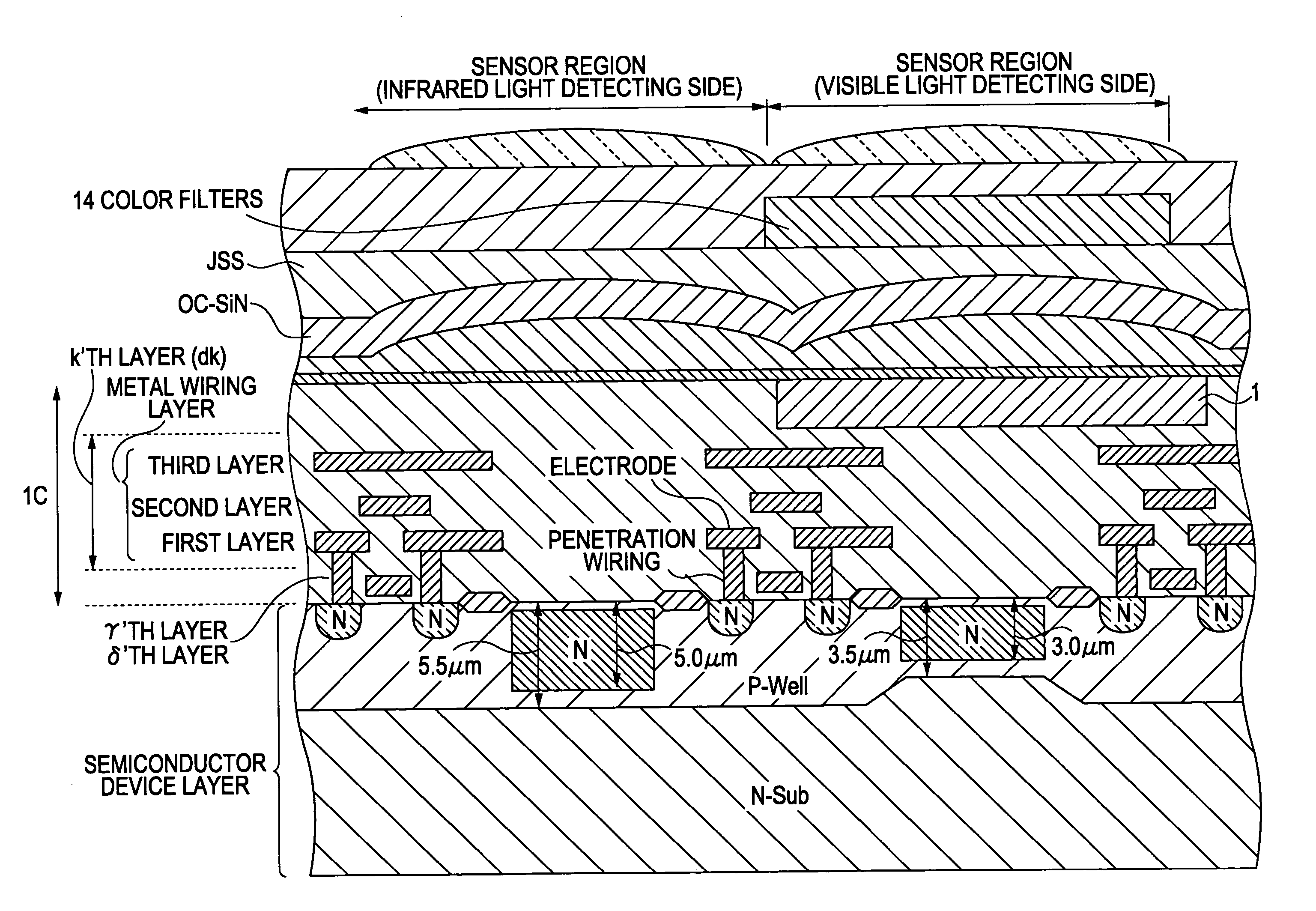
[0047] Description will be made in detail below regarding an embodiment of the present invention with reference to the drawings.

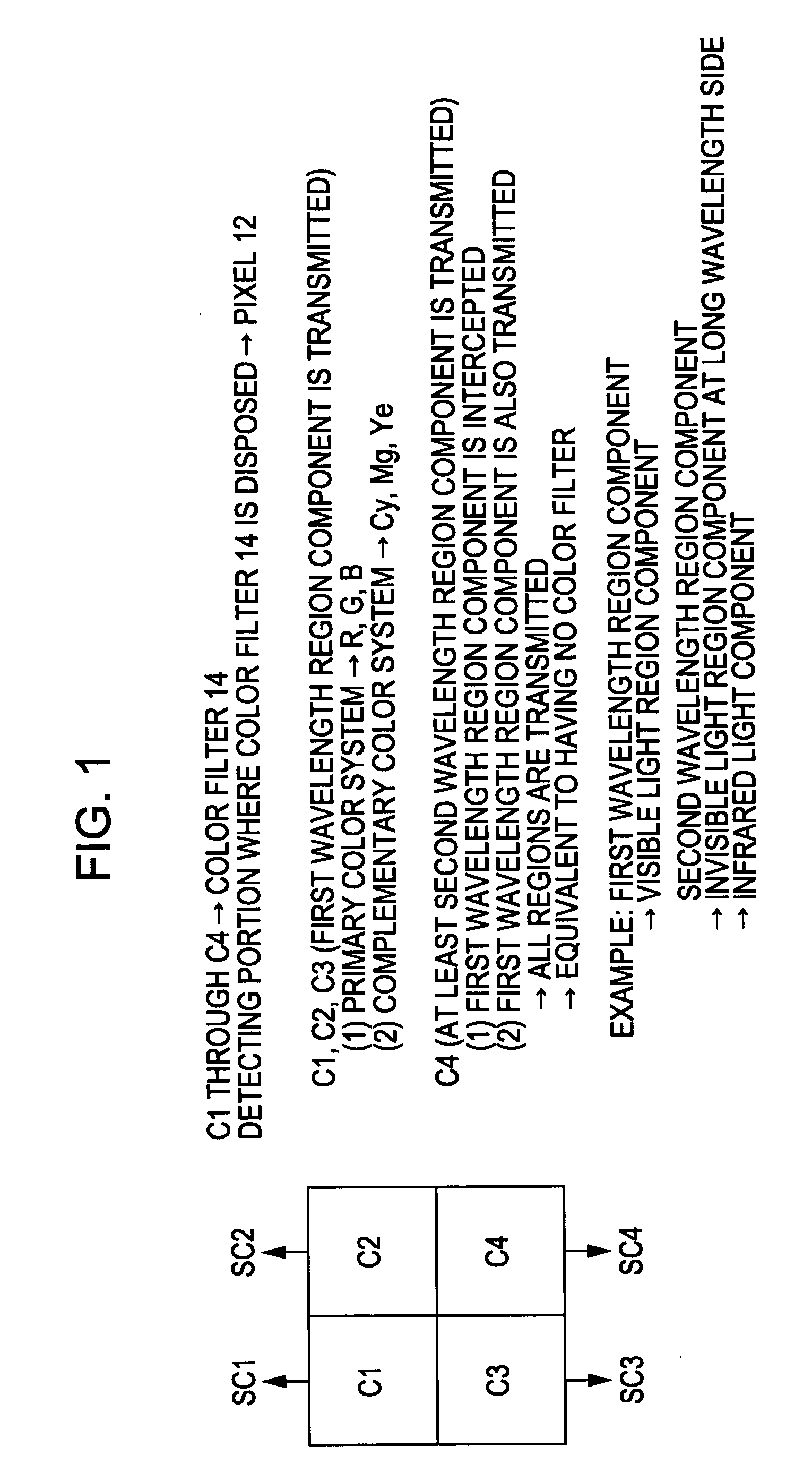
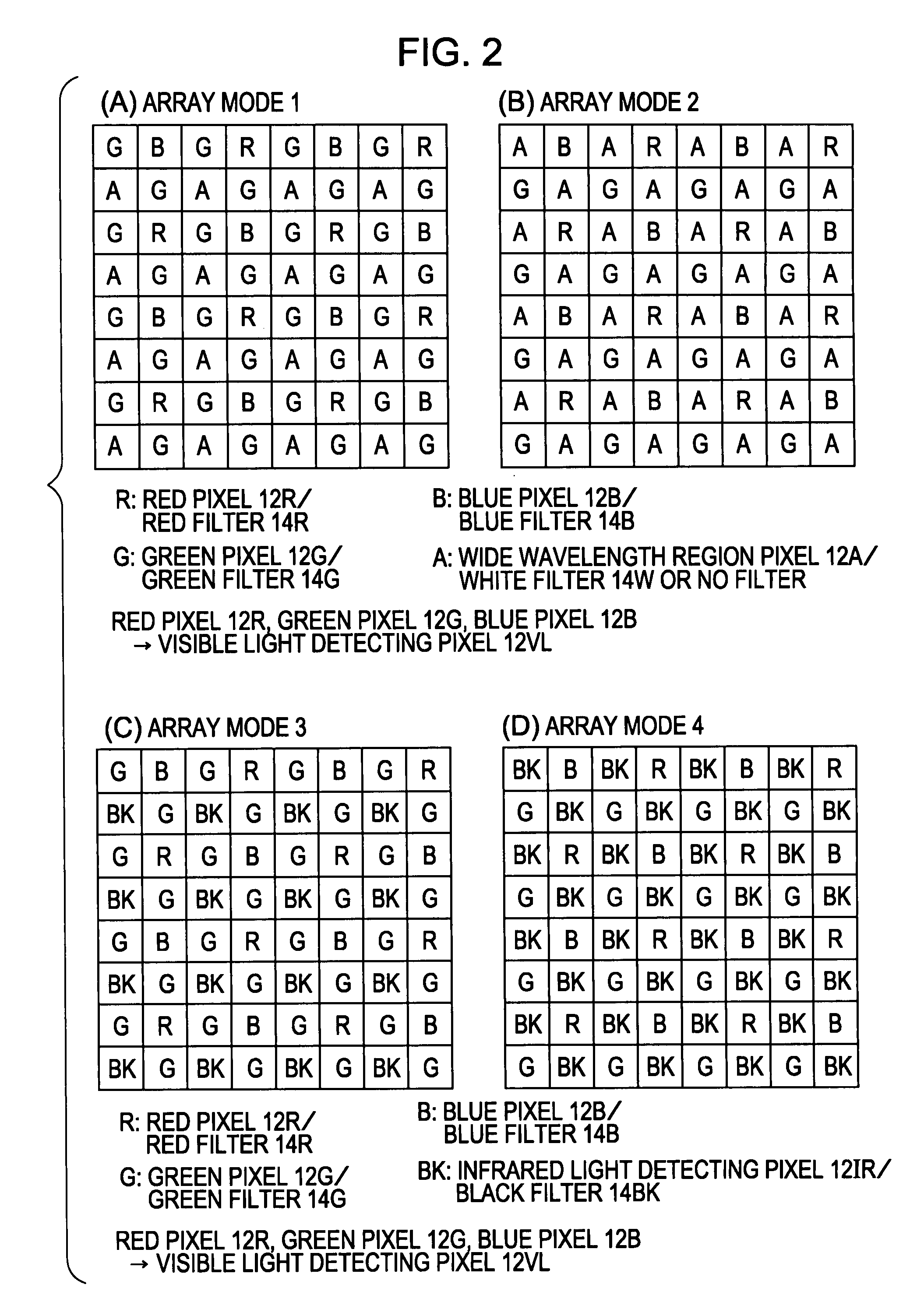
[0048]FIGS. 1 and 2 are diagrams illustrating color layout examples of color separation filters employed for the present embodiment. Here, FIG. 1 is a diagram illustrating the basic configuration of a color layout example of color separation filters, and FIG. 2 is a diagram illustrating one example as a specific example.

[0049] A color layout of color separation filters is basically a layout which always enables each of a visible color image and an infrared light image to be obtained independently. For example, as shown in FIG. 1, four types of color filters of color filters C1, C2, and C3 (each transmits a first wavelength region component which is a selectively specific wavelength region) for visible light color image which are filters for three wavelength regions (color components), and a color filter C4 having a different filter property from the color...


PUM


Abstract

A solid-state image capturing device, includes a semiconductor board, upon which same semiconductor board are disposed in a predetermined order: a first detecting unit for detecting a first wavelength region component within an electromagnetic wave; and a second detecting unit for detecting a second wavelength region component which is longer wavelength side than at least the first wavelength region component, wherein in the depth direction from the surface of the semiconductor board, a valid region where a first electroconductive type dopant of the second detecting unit is formed reaches a portion deeper than a valid region where a first electroconductive type dopant of the first detecting unit is formed.

Description

CROSS REFERENCES TO RELATED APPLICATIONS [0001] The present invention contains subject matter related to Japanese Patent Application JP 2006-272597 filed in the Japanese Patent Office on Oct. 4, 2006, the entire contents of which are incorporated herein by reference. BACKGROUND OF THE INVENTION [0002] 1. Field of the Invention [0003] The present invention relates to a solid-state image capturing device, an image capturing device, and a manufacturing method of a solid-state image capturing device. More specifically, the present invention relates to a signal obtaining technique which is suitable for being applied to a solid-state image capturing device or the like employing a physical amount distribution detecting semiconductor device wherein multiple unit components having sensitivity as to an electromagnetic wave input from the outside such as light, radiation, or the like, are arrayed, and a physical amount distribution converted into an electric signal by the unit components can b...

Claims


Application Information

Patent Timeline
IPC IPC(8): H01L31/0352H01L31/18H01L27/146H01L31/10H04N5/335H04N5/369H04N5/372H04N5/374
CPCH01L27/14603H01L27/14609H01L27/14621H01L27/14623H01L31/035281H01L27/14645H01L27/14649H01L27/14843H01L27/14627
Inventor TODA, ATSUSHI
Owner SONY CORP
Why Eureka
Try Eureka