
Nonvolatile memory device and method of fabricating the same

a memory device and non-volatile technology, applied in the direction of semiconductor devices, basic electric elements, electrical apparatus, etc., can solve the problems of short channel effect, loss of data, reduced electron injection efficiency, etc., to reduce misalignment, increase electron injection efficiency, and increase electron injection efficiency

Inactive Publication Date: 2008-04-17
SAMSUNG ELECTRONICS CO LTD +1
View PDF4 Cites 15 Cited by
  • Summary
  • Abstract
  • Description
  • Claims
  • Application Information

AI Technical Summary

Benefits of technology

[0008]It is therefore a feature of an embodiment of the present invention to provide a memory device having increased electron injection efficiency.
[0009]It is another feature of an embodiment of the present invention to provide a method of fabricating a memory device having increased electron injection efficiency and minimized misalignment.

Problems solved by technology

Volatile memory devices, e.g., dynamic random access memory (DRAM) and static random access memory (SRAM), may have fast data input / output characteristics but may lose data upon cutting off power supply.
However, the decreased size of the conventional unit cells in nonvolatile memory devices may reduce the length of the channel between the semiconductor substrate and the charge trap layer, thereby triggering a short channel effect and reduced electron injection efficiency.
Additionally, the conventional unit cells in nonvolatile memory devices may be produced by photo-etching, a process that may trigger misalignment thereof when the unit cells have decreased size.
In particular, the decreased size may generate misalignment of the charge trap layer and / or the control gate electrode, thereby deteriorating memory capabilities of the device and reducing the potential for high-degree integration of nonvolatile memory devices.

Method used


Image

  • Nonvolatile memory device and method of fabricating the same
  • Nonvolatile memory device and method of fabricating the same
  • Nonvolatile memory device and method of fabricating the same

Examples


Embodiment Construction

[0029]Korean Patent Application No. 10-2006-0100947 filed on Oct. 17, 2006, in the Korean Intellectual Property Office, and entitled: “Nonvolatile Memory Device and Method of Fabricating the Same,” is incorporated by reference herein in its entirety.

[0030]The present invention will now be described more fully hereinafter with reference to the accompanying drawings, in which exemplary embodiments of the invention are illustrated. The invention may, however, be embodied in different forms and should not be construed as limited to the embodiments set forth herein. Rather, these embodiments are provided so that this disclosure will be thorough and complete, and will fully convey the scope of the invention to those skilled in the art.

[0031]It will further be understood that when an element is referred to as being “on” another element, layer or substrate, it can be directly on the other element, layer or substrate, or intervening elements or layers may also be present. Further, it will be...


PUM


Abstract

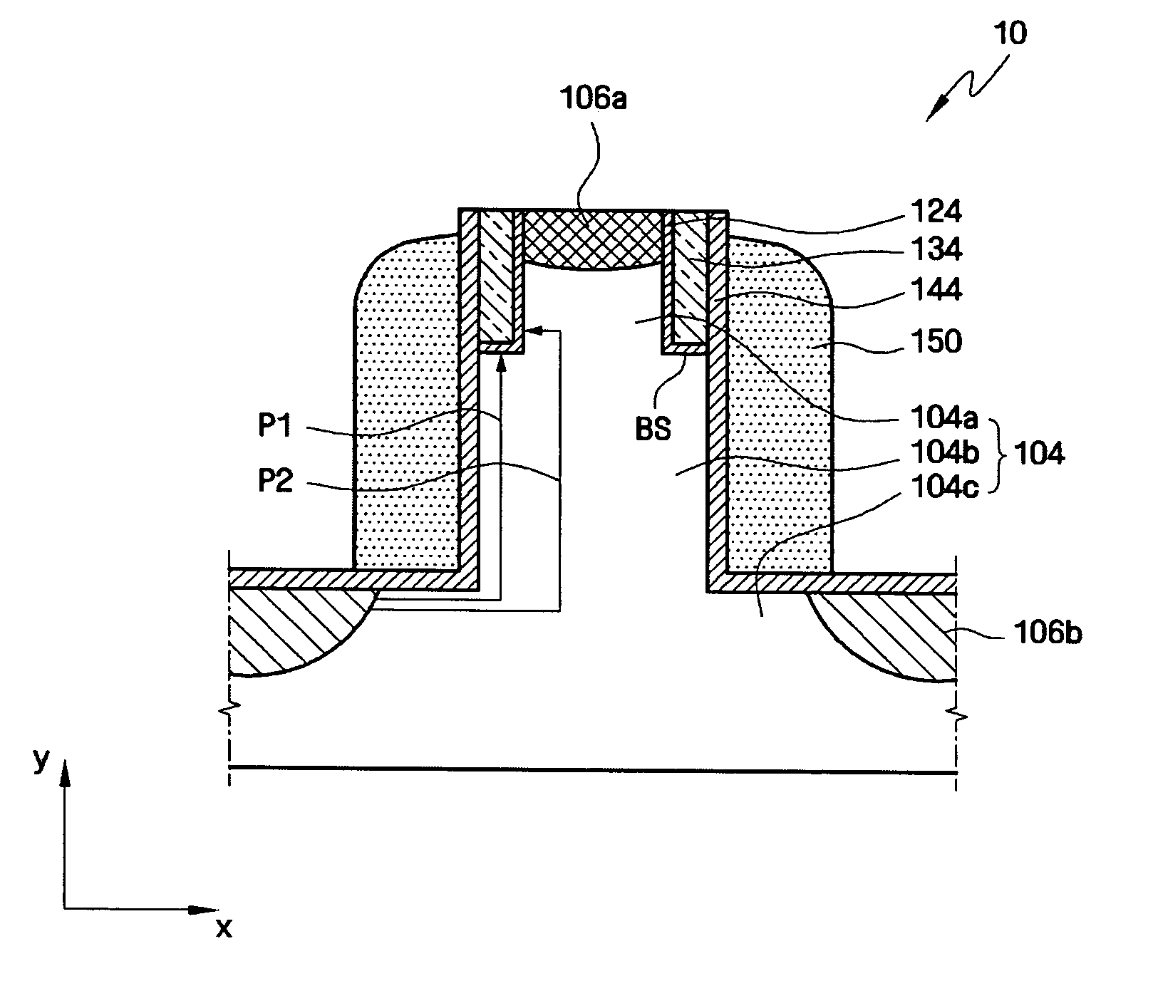
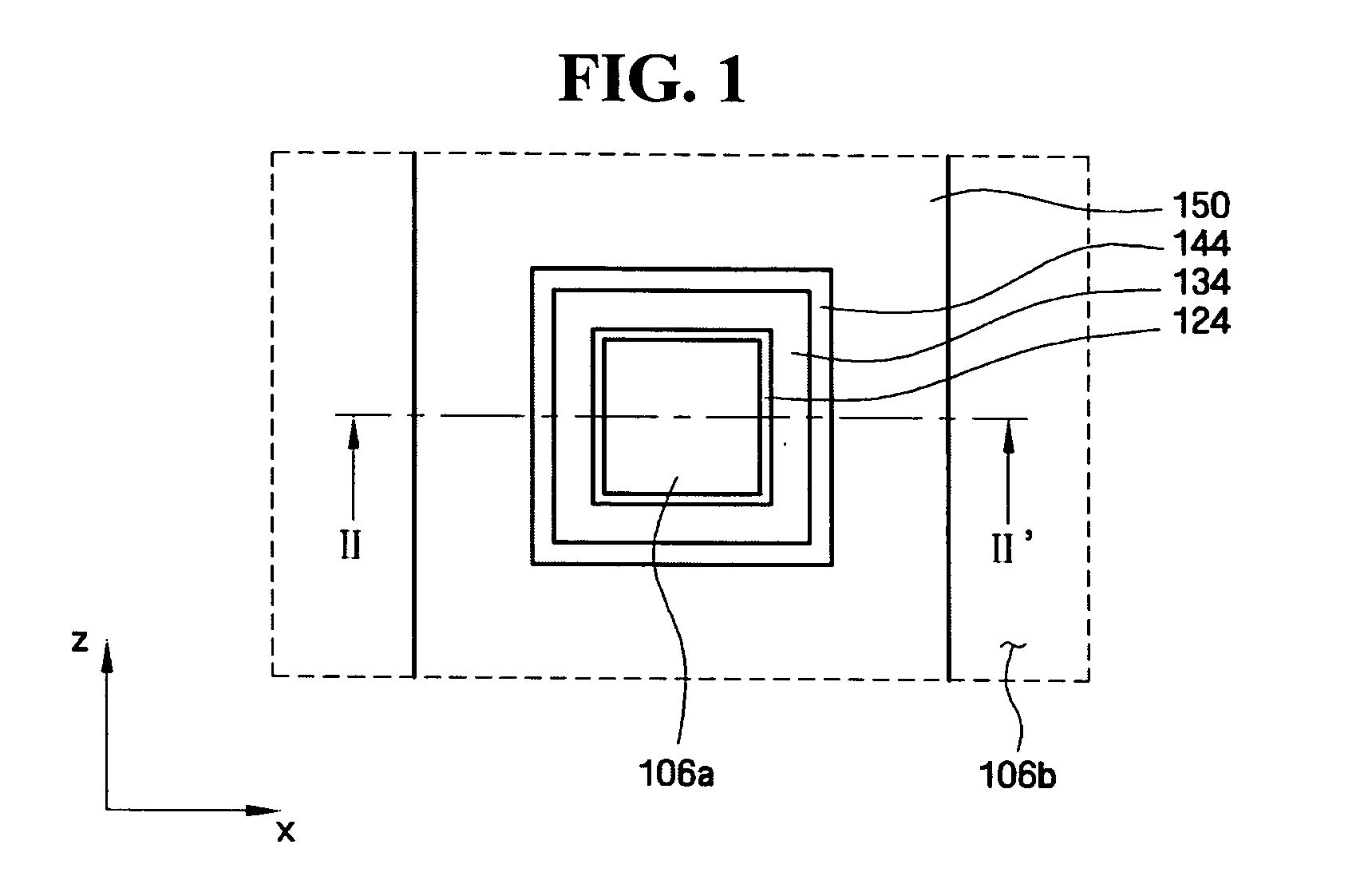
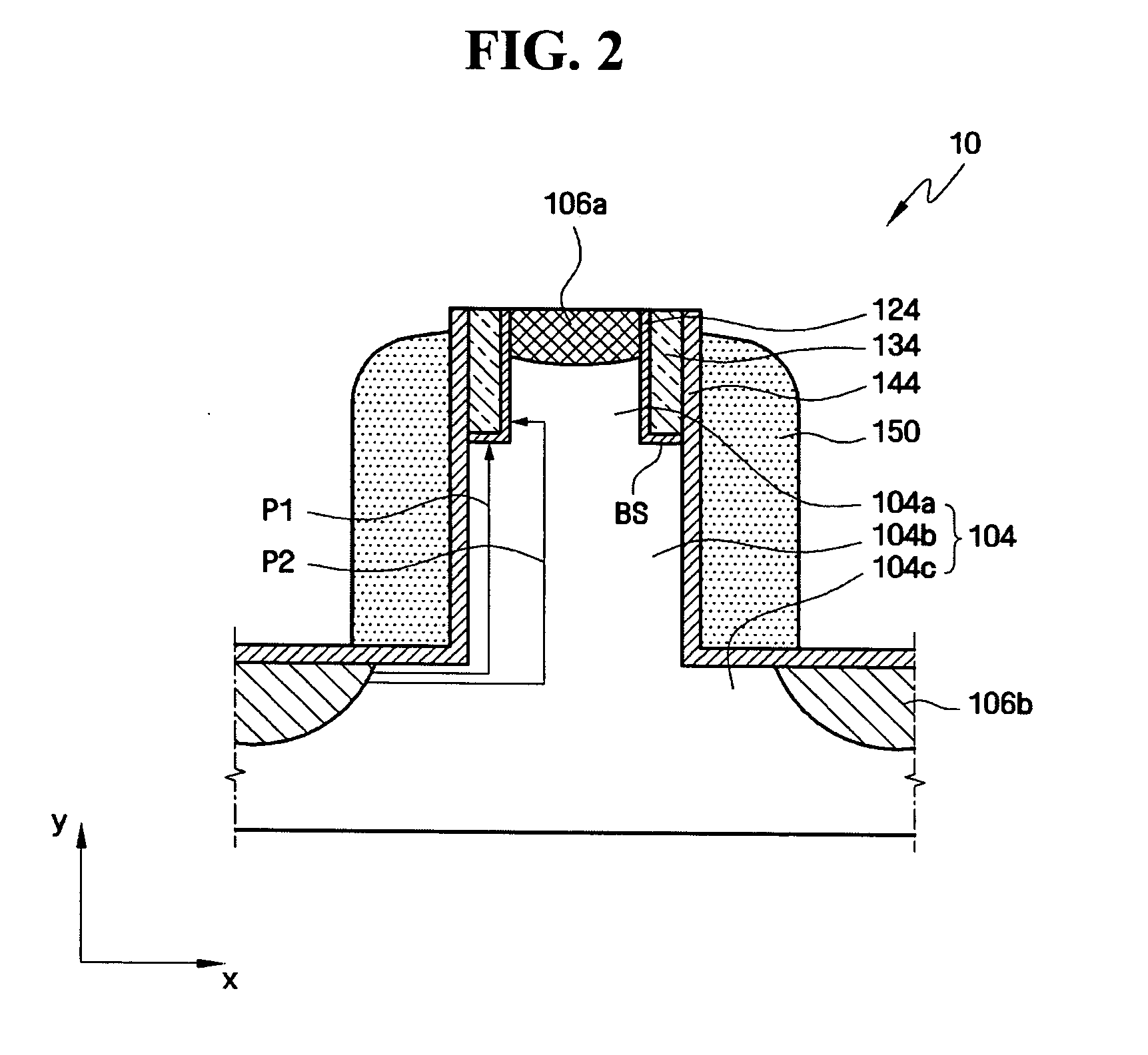
A nonvolatile memory device, includes a semiconductor substrate having a bottom part, a second vertical part positioned vertically on the bottom part, and a first vertical part having a width smaller than a width of the second vertical part and positioned on the second vertical part to have a boundary step therebetween; a charge trap layer disposed on a lateral surface of the first vertical part and on an upper surface of the boundary step; and a control gate electrode disposed on an upper surface of the bottom part and on lateral surfaces of the second vertical part and the charge trap layer.

Description

BACKGROUND OF THE INVENTION[0001]1. Field of the Invention[0002]The present invention relates to nonvolatile memory devices. In particular, the present invention relates to a nonvolatile memory device and a method of fabricating the same having increased electron injection efficiency and improved high integration capabilities.[0003]2. Description of the Prior Art[0004]In general, memory devices refer to semiconductor devices that can retain data, e.g., microcontrollers, credit cards, and so forth. Memory devices may be classified into volatile and non-volatile memory devices. Volatile memory devices, e.g., dynamic random access memory (DRAM) and static random access memory (SRAM), may have fast data input / output characteristics but may lose data upon cutting off power supply. Nonvolatile memory devices, e.g., read only memory (ROM), may have relatively slow data input / output characteristics but may retain the input data permanently.[0005]The conventional nonvolatile memory device, e...

Claims


Application Information

Patent Timeline
Patent Type & Authority Applications(United States)
IPC IPC(8): H01L29/792H01L21/8238H10B69/00
CPCH01L29/66833H01L29/7926H01L29/792H01L21/31144
Inventor CHAE, SOO-DOOKIM, CHUNG-WOOPARK, CHAN-JINHAN, JEONG-HEEPARK, BYUNG-GOOKPARK, IL-HAN
Owner SAMSUNG ELECTRONICS CO LTD
Learn More