Pattern forming apparatus, mark detecting apparatus, exposure apparatus, pattern forming method, exposure method, and device manufacturing method

a technology of pattern forming and mark detecting, applied in the direction of photomechanical equipment, instruments, optics, etc., can solve the problems of reducing the throughput of the exposure apparatus, the surface of the wafer is not always flat, and it is practically difficult to employ the measures of merely increasing the number of sample shots. , to achieve the effect of good precision, high integration and good accuracy

Active Publication Date: 2008-04-17
NIKON CORP
View PDF82 Cites 584 Cited by
  • Summary
  • Abstract
  • Description
  • Claims
  • Application Information

AI Technical Summary

Benefits of technology

[0069] With this method, while changing a relative positional relation between a plurality of mark detecting systems and the object mounted on the movable body in optical axis directions of the plurality of mark detecting systems that are perpendicular to the predetermined plan, simultaneously among the plurality of mark detecting systems, each of the marks formed at positions different from one another on the object is simultaneously detected, individually using each mark detecting system corresponding to each mark. Thus, by preferentially using each detection result of the mark, for example, in the most favorable focused state regarding

Problems solved by technology

Meanwhile, in a lithography process for manufacturing semiconductor devices or the like, multilayer circuit patterns are overlaid and formed on a wafer, and when the overlay accuracy between the layers is poor, the semiconductor devices or the like do not achieve predetermined circuit characteristics, which results in defectives in some cases.
Further, the wafer surf

Method used


Image

  • Pattern forming apparatus, mark detecting apparatus, exposure apparatus, pattern forming method, exposure method, and device manufacturing method
  • Pattern forming apparatus, mark detecting apparatus, exposure apparatus, pattern forming method, exposure method, and device manufacturing method
  • Pattern forming apparatus, mark detecting apparatus, exposure apparatus, pattern forming method, exposure method, and device manufacturing method

Examples


Embodiment Construction

[0126] An embodiment of the present invention will be described below, with reference to FIGS. 1 to 36.

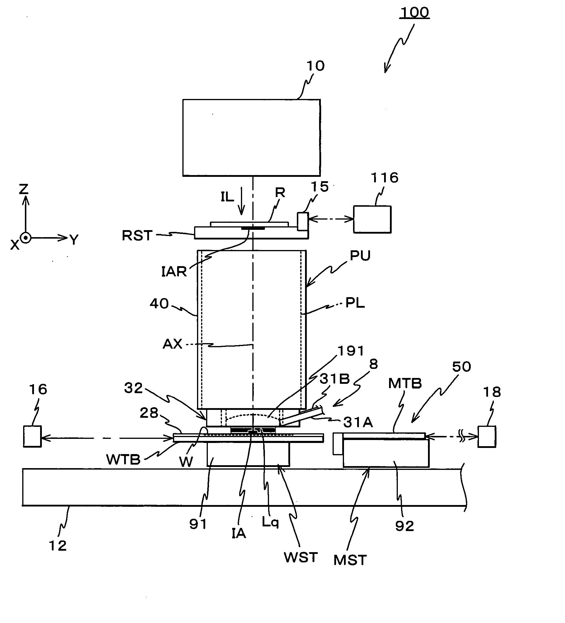
[0127]FIG. 1 schematically shows the configuration of an exposure apparatus 100 related to an embodiment. Exposure apparatus 100 is a scanning exposure apparatus by a step-and-scan method, that is, a so-called scanner. As will be described later, in the embodiment, a projection optical system PL is arranged, and the following description will be made assuming that a direction parallel to an optical axis AX of projection optical system PL is a Z-axis direction, a direction in which a reticle and a wafer are relatively scanned within a plane orthogonal to the Z-axis direction is a Y-axis direction and a direction that is orthogonal to a Z-axis and a Y-axis is an X-axis direction, and rotation (tilt) directions around the X-axis, the Y-axis and the Z-axis are θx, θy and θz directions respectively.

[0128] Exposure apparatus 100 is equipped with an illumination system 10, a reticle sta...


PUM

PropertyMeasurementUnit
Timeaaaaaaaaaa
Timeaaaaaaaaaa
Areaaaaaaaaaaa

Abstract

While a wafer stage linearly moves in a Y-axis direction, a multipoint AF system detects surface position information of the wafer surface at a plurality of detection points that are set at a predetermined distance in an X-axis direction and also a plurality of alignment systems that are arrayed in a line along the X-axis direction detect each of marks at positions different from one another on the wafer. That is, detection of surface position information of the wafer surface at a plurality of detection points and detection of the marks at positions different from one another on the wafer are finished, only by the wafer stage (wafer) linearly passing through the array of the plurality of detection points of the multipoint AF system and the plurality of alignment systems, and therefore, the throughput can be improved, compared with the case where a detection operation of the marks and a detection operation of the surface position information (focus information) are independently performed.

Description

CROSS-REFERENCE TO RELATED APPLICATIONS [0001] This non-provisional application claims the benefit of Provisional Application No. 60 / 780,049 filed Mar. 8, 2006, the disclosure of which is hereby incorporated herein by reference in its entirety.BACKGROUND OF THE INVENTION [0002] 1. Field of the Invention [0003] The present invention relates to pattern forming apparatuses, mark detecting apparatuses, exposure apparatuses, pattern forming methods, exposure methods and device manufacturing methods, and more particularly to a pattern forming apparatus and an exposure apparatus that are used when manufacturing electron devices such as semiconductor devices and liquid crystal display devices, or the like, a mark detecting apparatus that can suitably be used in the pattern forming apparatus or the exposure apparatus, a pattern forming method and an exposure method that can suitably be used when manufacturing the electron devices, and a device manufacturing method in which the pattern formin...

Claims


Application Information

Patent Timeline
IPC IPC(8): G01B11/00
CPCG03F9/7003G03F9/7026Y10T29/49826G03F2009/005G03F9/7088G03F7/70341G03F7/70641G03F7/70666G03F7/706G03F7/70616H01L21/0274H01L21/027G03F7/70491G03F7/70775G03F7/70725
Inventor SHIBAZAKI, YUICHI
Owner NIKON CORP
Why Eureka
Try Eureka