

Aligned crystalline semiconducting film on a glass substrate and method of making
a technology of aligned crystalline semiconducting film and glass substrate, which is applied in the field of semiconducting structure having a glass substrate, can solve the problems of inability to use epitaxial templates directly in conventional epitaxial growth processes, limited selection of materials and sizes, and single crystal templates used in conventional epitaxial growth techniques
- Summary
- Abstract
- Description
- Claims
- Application Information
AI Technical Summary
Problems solved by technology
Method used
Image

Examples
example 1
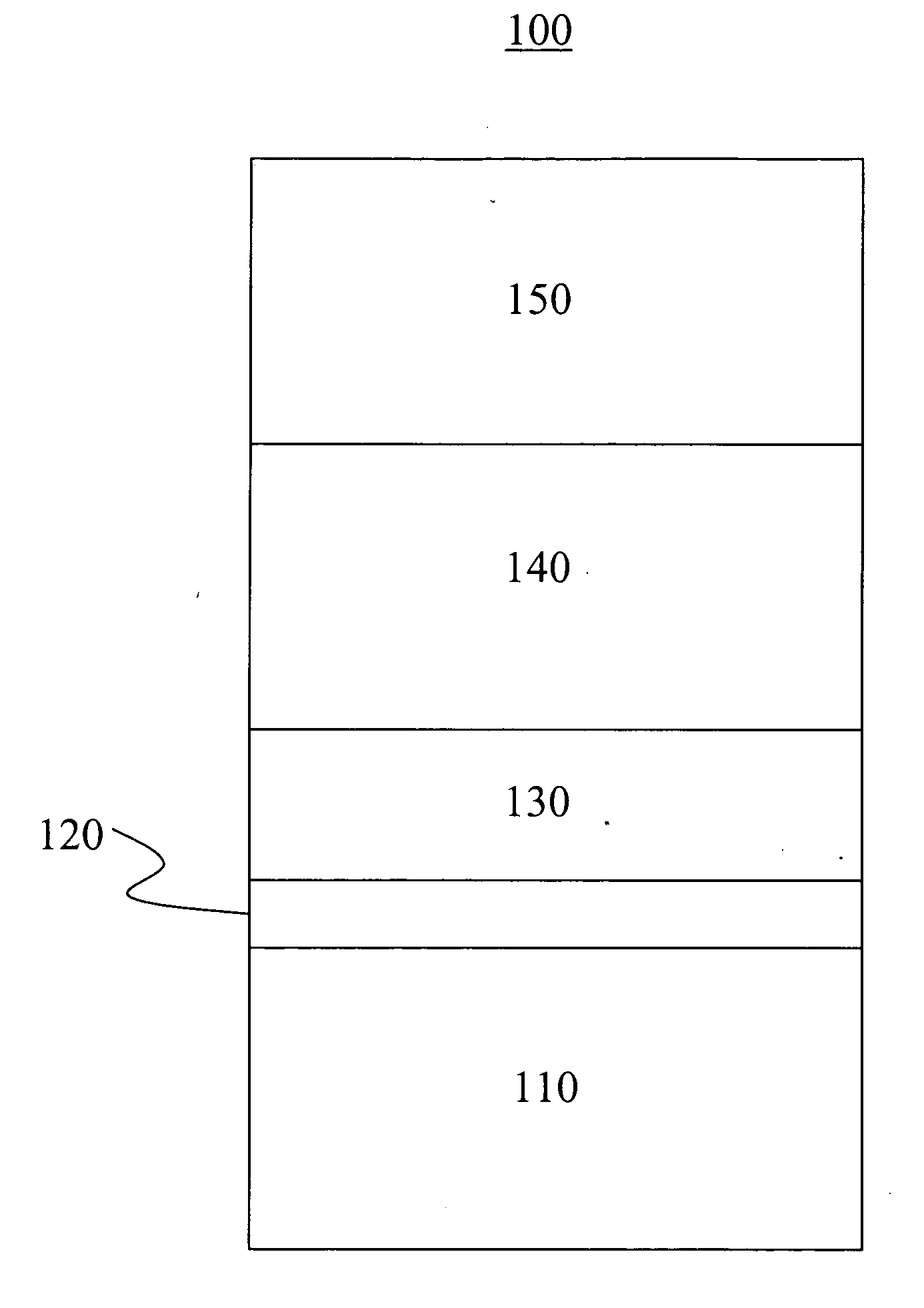
[0035]Biaxially oriented silicon films were grown on buffered glass substrates as follows. Substrates consisting of Corning Eagle 2000™ glass, having dimensions of 10 mm length×10 mm width×0.7 mm thickness, were ultrasonically cleaned in isopropanol. The back side of each glass substrate was painted with carbon paint to allow for uniform and stable heating by quartz lamps during multi-layer film growth. The cleaned and painted glass substrates were clipped to carriers in a reel-to-reel system with the painted side exposed to direct quartz lamp light during heating. Throughout the deposition process, heating and cooling was done slowly (˜50° C. / min above 550° C.).
[0036]The surfaces of the glass substrates were ion-sputtered to create texture on the glass substrate to serve as a nucleation layer for the subsequent IBAD growth. Using a 6 cm×22 cm rf ion source, the glass substrate was exposed to 750 eV / 30 mA Ar+ ions for about 15 minutes to form the nucleation layer. The ion beam was d...
example 2
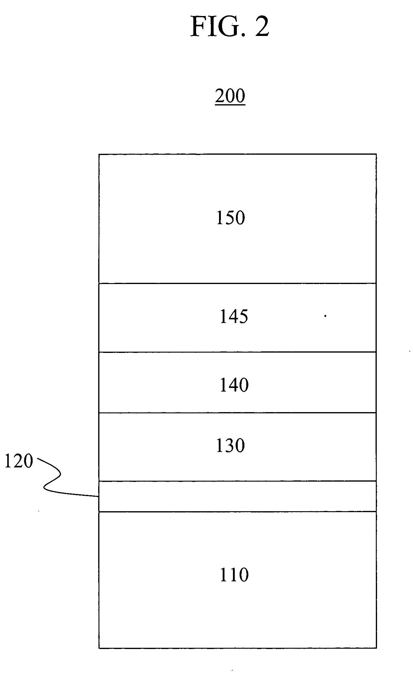
[0041]Biaxially oriented silicon films were grown on buffered glass substrates as follows. Substrates consisting of Corning Eagle 2000™ glass, having dimensions of 10 mm length×10 mm width×0.7 mm thickness, were ultrasonically cleaned in isopropanol. The back side of each glass substrate was painted with carbon paint to allow for uniform and stable heating by quartz lamps during multi-layer film growth. The cleaned and painted glass substrates were clipped to carriers in a reel-to-reel system with the painted side exposed to direct quartz lamp light during heating. Throughout the deposition process, heating and cooling was done slowly (˜50° C. / min above 550° C.).
[0042]The glass substrate was exposed to 750 eV / 30 mA Ar+ ions for about 1 minute to remove hydrocarbons and other types of residues from the surface of the glass substrate. The ion beam was directed at 45 degrees to the substrate normal.
[0043]Silicon oxide was deposited using e-beam evaporation to serve as a nucleation laye...
example 3
[0048]Biaxially oriented silicon films were grown on buffered glass substrates as follows. Substrates consisting of Corning Eagle 2000™ glass, having dimensions of 10 mm length×10 mm width×0.7 mm thickness, were ultrasonically cleaned in isopropanol. The back side of each glass substrate was painted with carbon paint to allow for uniform and stable heating by quartz lamps during multi-layer film growth. The cleaned and painted glass substrates were clipped to carriers in a reel-to-reel system with the painted side exposed to direct quartz lamp light during heating. Throughout the deposition process, heating and cooling was done slowly (˜50° C. / min above 550° C.).
[0049]The glass substrate was exposed to 750 eV / 30 mA Ar+ ions for about 1 minute to remove hydrocarbons and other types of residues from the surface of the glass substrate. The ion beam was directed at 45 degrees to the substrate normal.
[0050]Silicon nitride was deposited using e-beam evaporation to serve as a nucleation la...
PUM
| Property | Measurement | Unit |
|---|---|---|
| softening temperature | aaaaa | aaaaa |
| thickness | aaaaa | aaaaa |
| thickness | aaaaa | aaaaa |
Abstract
Description
Claims
Application Information