

Method of manufacturing semiconductor device
a manufacturing method and semiconductor technology, applied in the direction of semiconductor devices, electrical devices, transistors, etc., can solve the problem of difficult to suppress the growth of nisisub>2 /sub>crystals in spikes
- Summary
- Abstract
- Description
- Claims
- Application Information
AI Technical Summary
Problems solved by technology
Method used
Image

Examples
first embodiment
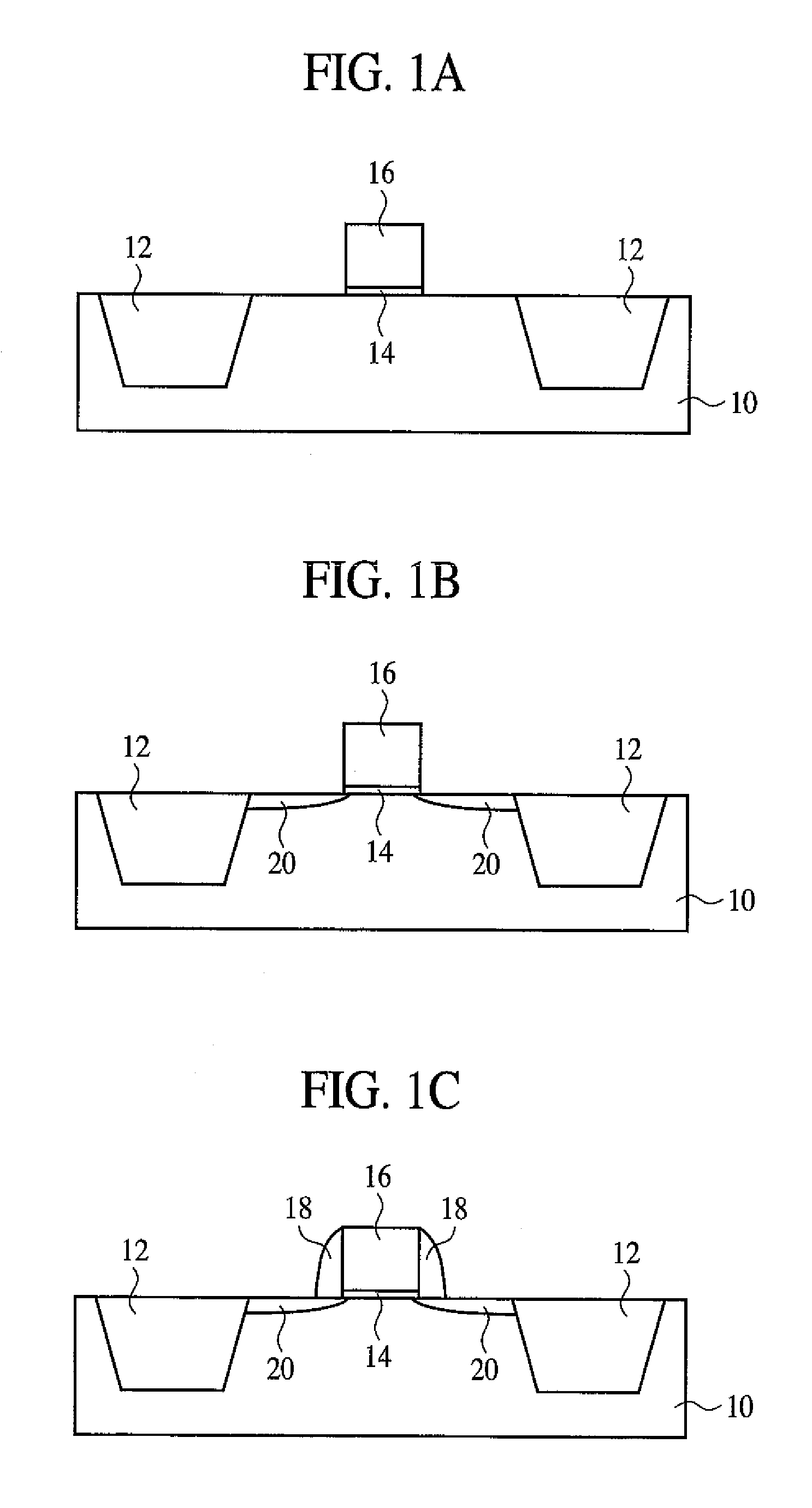
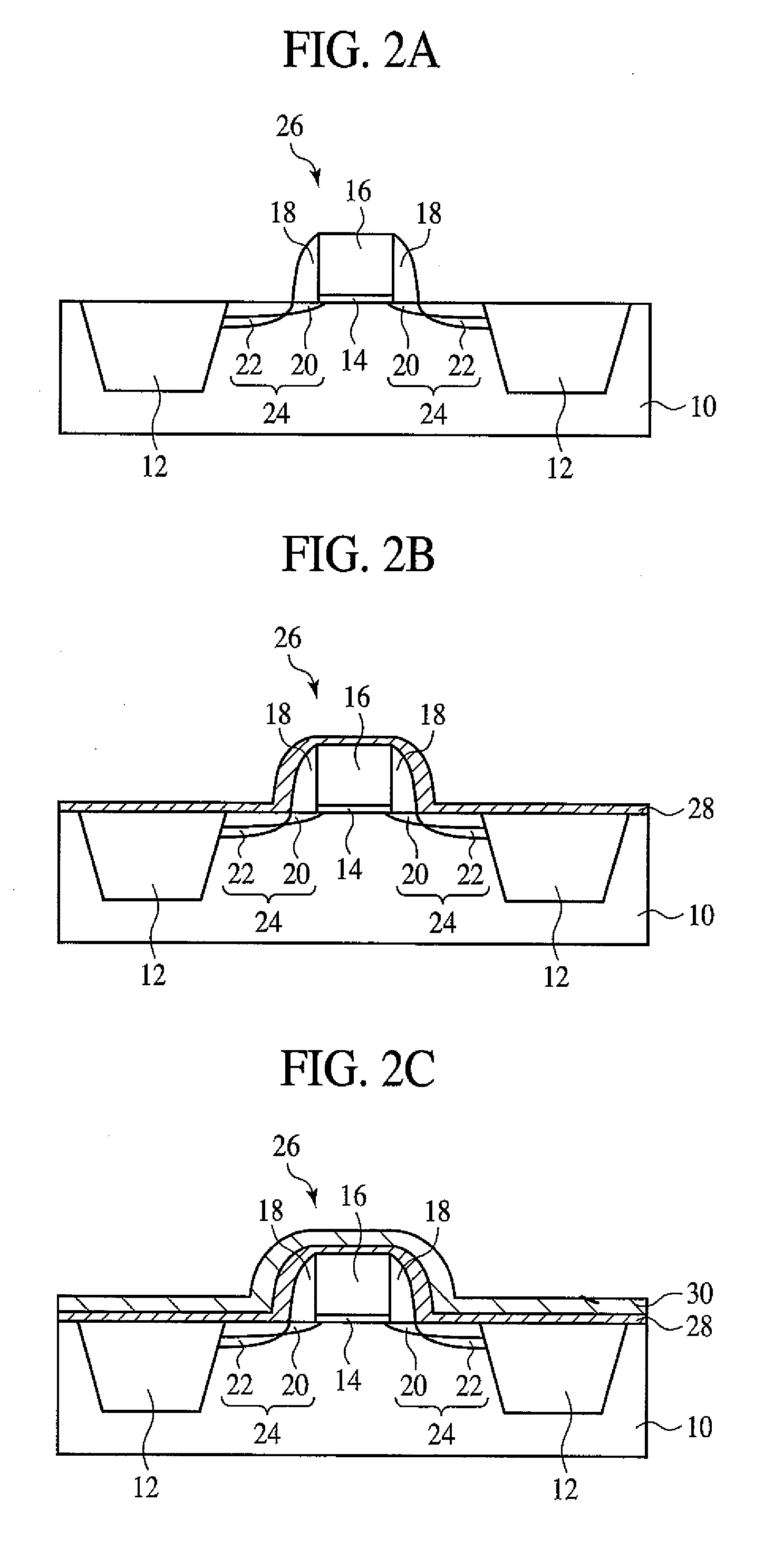
A First Embodiment
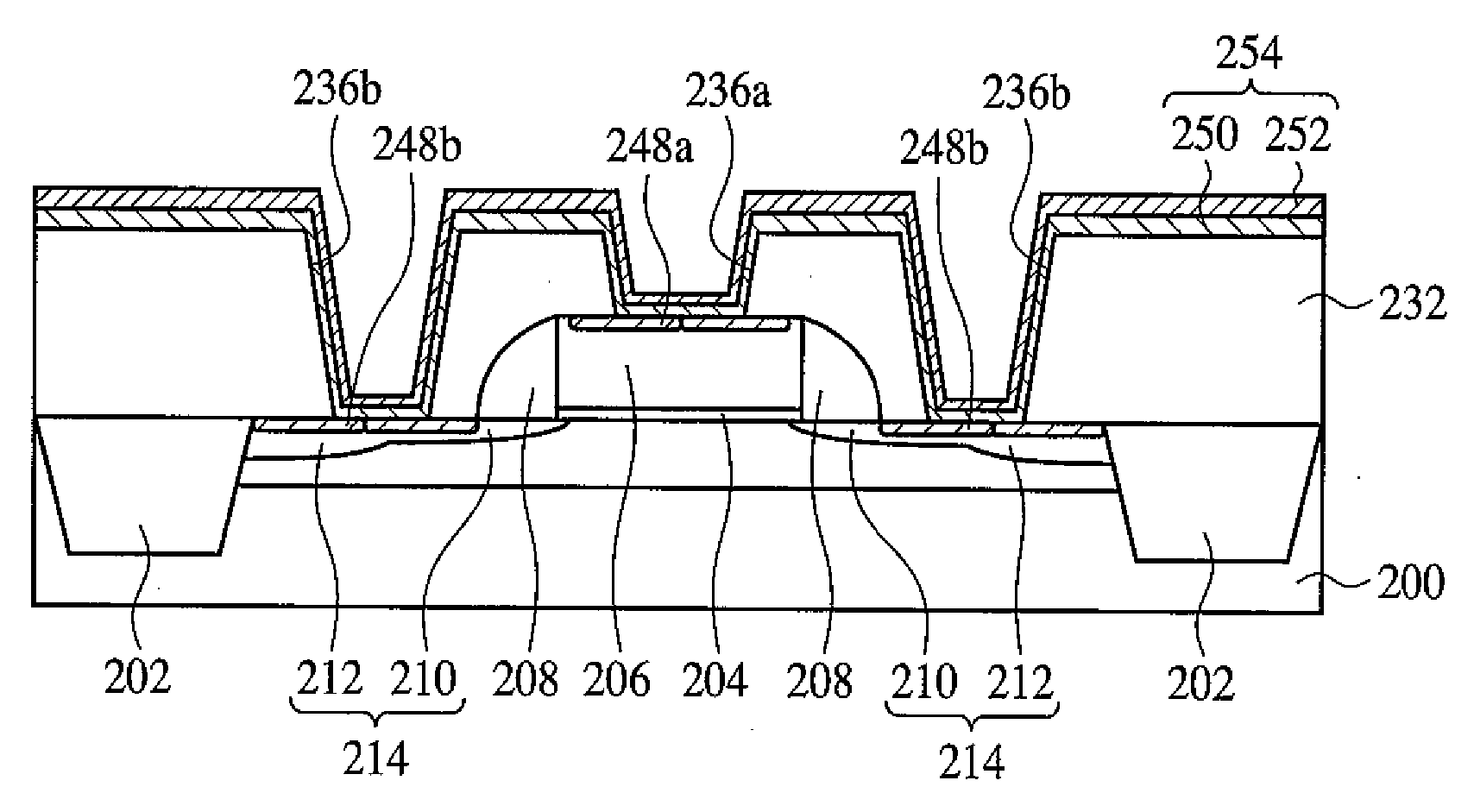
[0075] Before the method of manufacturing the semiconductor device according to the present invention is explained, the silicidation process using a nickel platinum (NiPt) film will be explained with reference to FIGS. 47A-47C, 48A-48B and 49A-49C.
[0076]FIGS. 47A-48C and 48A-48B are sectional views showing the steps of a proposed method of manufacturing a semiconductor device (Part 1).
[0077] First, on a silicon substrate 200, a MOS transistor 216 including a gate electrode 206 and source / drain diffused layers 214 is formed by the usual MOS transistor manufacturing method.
[0078]FIG. 47A illustrates the MOS transistor formed on the silicon substrate 200. As illustrated, a device region is defined by a device isolation region 202 on the semiconductor substrate 200. On the silicon substrate 200 with the device region defined, the gate electrode 206 of a polysilicon film is formed with a gate insulating film 204 formed therebetween. A sidewall insulating film 208 is ...
second embodiment
A Second Embodiment
[0192] The method of manufacturing the semiconductor device according to a second embodiment of the present invention will be explained with reference to FIGS. 15A to 18B. FIGS. 15A-15C, 16A-16C, 17A-17C and 18A-18B are sectional views showing the steps of the method of manufacturing the semiconductor device according to the present embodiment. The same members of the present embodiment as those of the method of manufacturing the semiconductor device according to the first embodiment are represented by the same reference numbers not to repeat or to simplify their explanation.
[0193] The method of manufacturing the semiconductor device according to the present embodiment is characterized mainly in that compressive strain is introduced into the channel region of a PMOS transistor.
[0194] First, in the same way as in the method of manufacturing the semiconductor device according to the first embodiment shown in FIGS. 1A and 1B, in an NMOS transistor-to-be-formed regi...
third embodiment
A Third Embodiment
[0241] The method of manufacturing the semiconductor device according to a third embodiment of the present invention will be explained with reference to FIGS. 20A to 22B. FIGS. 20A-20C, 21A-21C and 22A-22B are sectional views showing the steps of the method of manufacturing the semiconductor device according to the present embodiment. The same members of the present embodiment as those of the method of manufacturing the semiconductor device according to the first and the second embodiments are represented by the same reference numbers not to repeat or to simplify their explanation.
[0242] The method of manufacturing the semiconductor device according to the present embodiment is characterized mainly in that tensile strain is introduced into the channel region of an NMOS transistor.
[0243] In the same way as in the method of manufacturing the semiconductor device according to the second embodiment shown in FIG. 15A to FIG. 16A, in an NMOS transistor-to-be-formed reg...
PUM
| Property | Measurement | Unit |
|---|---|---|
| temperature | aaaaa | aaaaa |
| temperature | aaaaa | aaaaa |
| temperature | aaaaa | aaaaa |
Abstract
Description
Claims
Application Information