Roll-To-Roll Electroplating for Photovoltaic Film Manufacturing

a photovoltaic film and electroplating technology, applied in the direction of electrolysis components, sustainable manufacturing/processing, final product manufacturing, etc., can solve the problems of high plating current density, non-uniformity, and problems of adhesion to the substrate, so as to reduce the effective series resistance of the device

Inactive Publication Date: 2008-04-24
SOLOPOWER
View PDF16 Cites 61 Cited by
  • Summary
  • Abstract
  • Description
  • Claims
  • Application Information

AI Technical Summary

Benefits of technology

[0005] The structure of a conventional Group IBIIIAVIA compound photovoltaic cell such as a Cu(In,Ga,Al)(S,Se,Te)2 thin film solar cell is shown in FIG. 1. The device 10 is fabricated on a substrate 11, such as a sheet of glass, a sheet of metal (such as aluminum or stainless steel), an insulating foil or web, or a conductive foil or web. The absorber film 12, which comprises a material in the family of Cu(In,Ga,Al)(S,Se,Te)2, is grown over a conductive layer 13, which is previously deposited on the substrate 11 and which acts as the electrical contact to the device. Various conductive layers comprising Mo, Ta, W, Ti, and stainless steel etc. have been used in the solar cell structure of FIG. 1. If the substrate itself is a properly selected conductive material, it is possible not to use a conductive layer 13, since the substrate 11 may then be used as the ohmic contact to the device. After the absorber film 12 is grown, a transparent layer 14 such as a CdS, ZnO or CdS / ZnO stack is formed on the absorber film. Radiation 15 enters the device through the transparent layer 14. Metallic grids (not shown) may also be deposited over the transparent layer 14 to reduce the effective series resistance of the device. It should be noted that the structure of FIG. 1 may also be inverted if substrate is transparent. In that case light enters the device from the substrate side of the solar cell.

Problems solved by technology

However, the cost of electricity generated using silicon-based solar cells is higher than the cost of electricity generated by the more traditional methods.
This technique was found to require very high plating current densities resulting in non-uniformities and problems of adhesion to the substrate as discussed in reference publications (Kapur et al., “Low Cost Thin Film Chalcopyrite Solar Cells, Proceedings of 18th IEEE Photovoltaic Specialists Conf., 1985, p.

Method used


Image

  • Roll-To-Roll Electroplating for Photovoltaic Film Manufacturing
  • Roll-To-Roll Electroplating for Photovoltaic Film Manufacturing
  • Roll-To-Roll Electroplating for Photovoltaic Film Manufacturing

Examples


Embodiment Construction

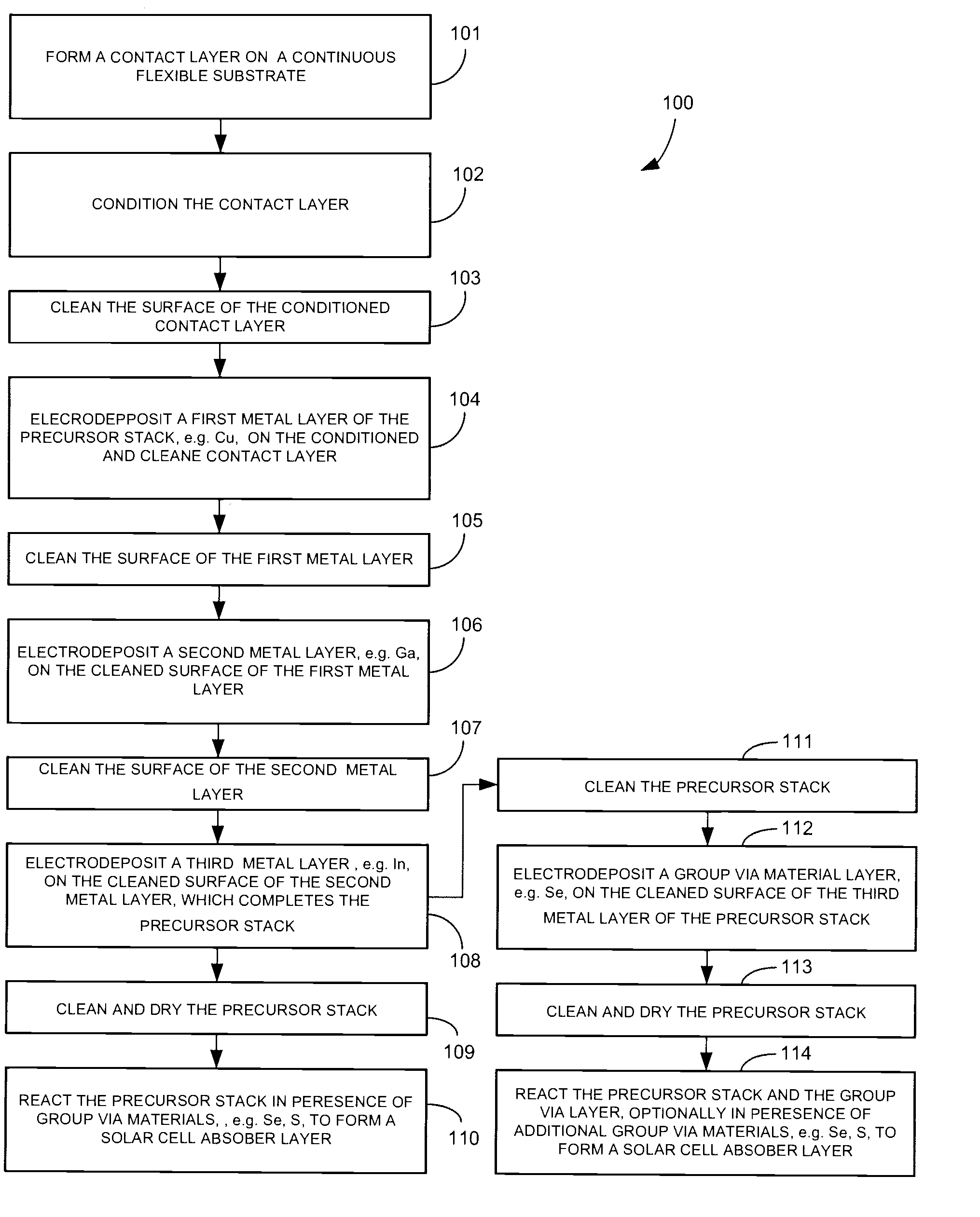
[0023] Present invention provides a low-cost, high throughput two-stage process for fabrication of CIGS(S) type absorber layers for manufacturing of solar cells.

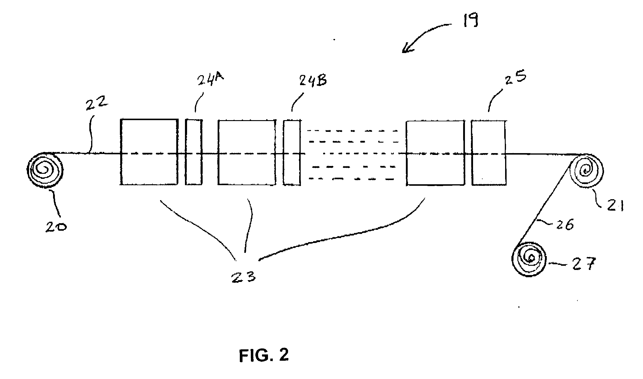
[0024]FIG. 2 schematically shows an embodiment of the process and the tool of the present invention. In this embodiment, a roll-to-roll processing technique is used to electrodeposit a Group IB material (preferably Cu) and a Group IIIA material (preferably at least one of In and Ga) in a continuous manner on a continuous flexible workpiece 22 such as a flexible foil base including a flexible substrate and a contact layer. The tool 19 has a supply spool 20 and a return spool 21 and the flexible foil base 22 is directed from the supply spool 20 to the return spool 21 through a series of electroplating units 23. The process units 23 may include at least one Group IB material electroplating unit, and at least one Group IIIA material electroplating unit. After each electroplating unit 23, there may preferably be cleaning units 2...


PUM

PropertyMeasurementUnit
molar ratioaaaaaaaaaa
molar ratiosaaaaaaaaaa

Abstract

A roll to roll system for forming an absorber structure for solar cells on a flexible foil as the flexible foil is advanced through units of the system and by unwrapping from a supply spool and wrapping around a take-up spool. Surface of the flexible foil is first conditioned in a conditioning unit to form an activated surface. A precursor stack including copper, gallium and indium layers is electroplated onto the activated surface by utilizing separate electroplating units for each layers. The precursor layer is reacted with at least one of Se and S in an annealing unit of the system.

Description

CROSS REFERENCE TO RELATED APPLICATIONS [0001] This application claims priority to Provisional Application Ser. No. 60 / 862,164 filed on Oct. 19, 2006.FIELD OF THE INVENTION [0002] The present invention relates to methods and apparatus for preparing thin films of Group IBIIIAVIA compound semiconductor films for radiation detector and photovoltaic applications. BACKGROUND [0003] Solar cells are photovoltaic devices that convert sunlight directly into electrical power. The most common solar cell material is silicon, which is in the form of single or polycrystalline wafers. However, the cost of electricity generated using silicon-based solar cells is higher than the cost of electricity generated by the more traditional methods. Therefore, since early 1970's there has been an effort to reduce cost of solar cells for terrestrial use. One way of reducing the cost of solar cells is to develop low-cost thin film growth techniques that can deposit solar-cell-quality absorber materials on larg...

Claims


Application Information

Patent Timeline
Patent Type & Authority Applications(United States)
IPC IPC(8): C25D5/10C25D17/00
CPCC25D5/10C25D5/50C25D7/0635Y02E10/541C25D21/12H01L31/0322H01L31/03928C25D17/00Y02P70/50H01L31/18H01L31/04B82Y30/00
Inventor BASOL, BULENT M.
Owner SOLOPOWER
Why Eureka
Try Eureka