Apparatus and method for CDS and ADC with multiple samplings in image sensor

a technology of image sensor and apparatus, applied in the field of apparatus and method for cds and adc with multiple samplings in image sensor, can solve problems such as serious degrade image quality, and achieve the effect of reducing random nois

Active Publication Date: 2008-04-24
SAMSUNG ELECTRONICS CO LTD
View PDF5 Cites 31 Cited by
  • Summary
  • Abstract
  • Description
  • Claims
  • Application Information

AI Technical Summary

Benefits of technology

[0031] In this manner, the reset and image signals are sampled multiple times, and the result of the CDS and ADC are summed together for reducing random noise. In addition, such multiple samplings and processing of such multiple samplings are performed within the horizontal scan time period for retaining speed performance of the image sensor.

Problems solved by technology

Such increased random noise may seriously degrade image quality in the CIS 10.

Method used


Image

  • Apparatus and method for CDS and ADC with multiple samplings in image sensor
  • Apparatus and method for CDS and ADC with multiple samplings in image sensor
  • Apparatus and method for CDS and ADC with multiple samplings in image sensor

Examples


Embodiment Construction

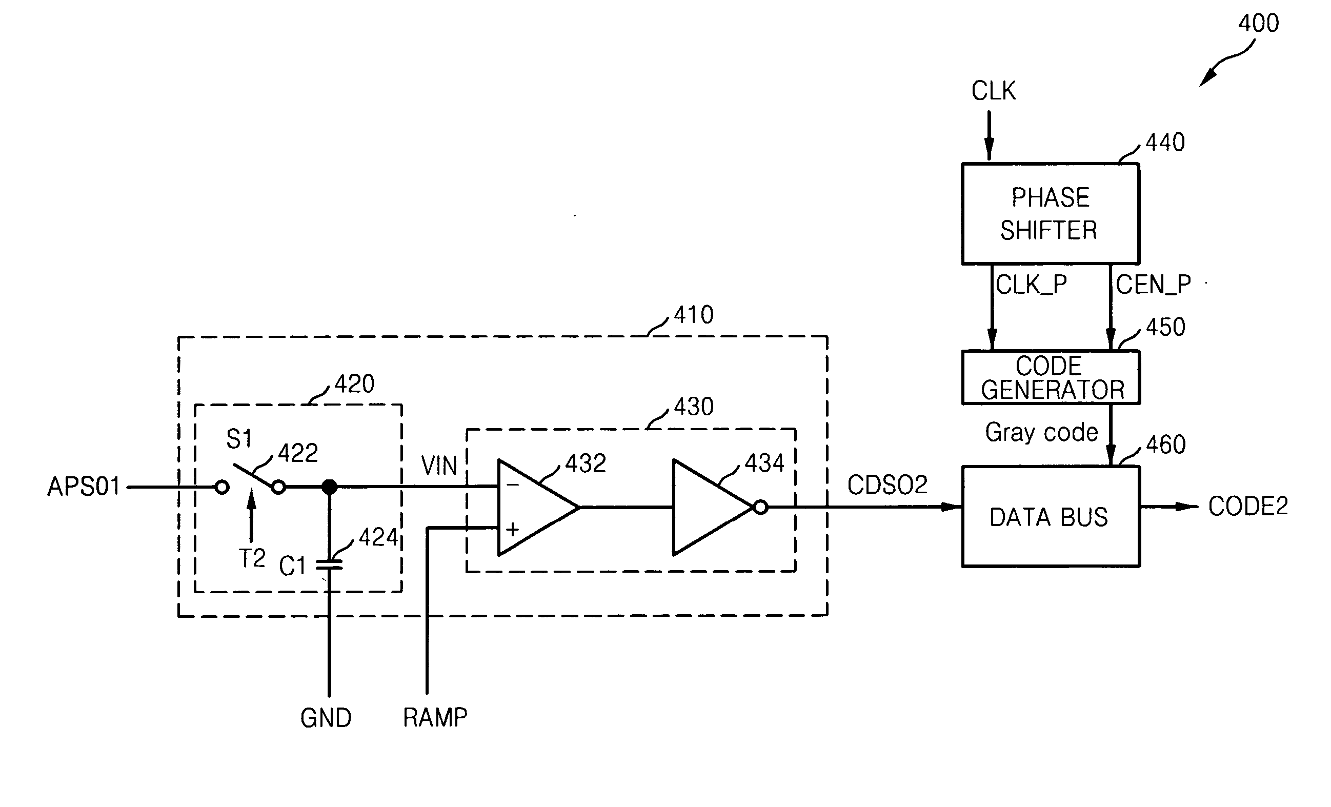
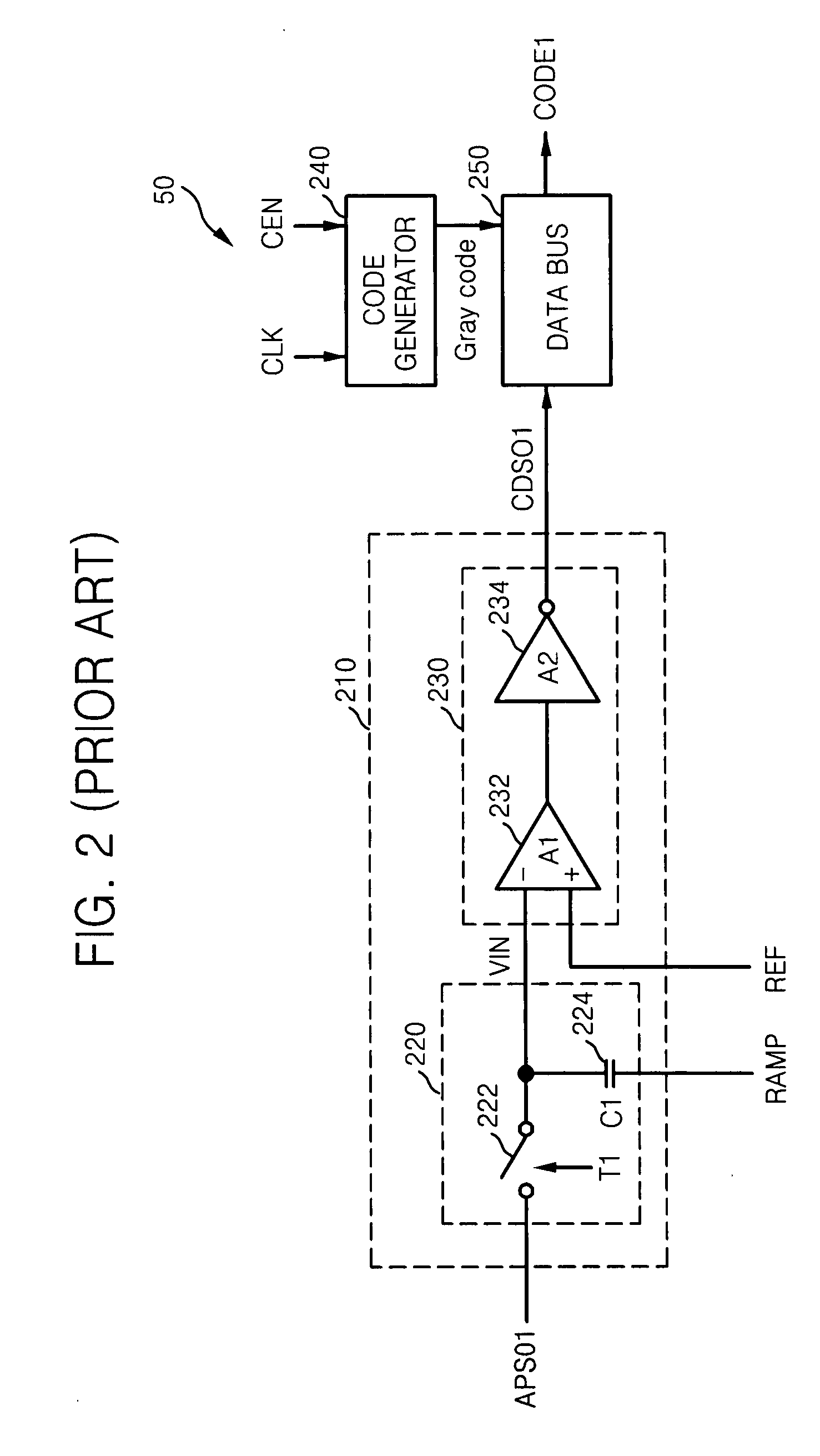
[0047]FIG. 4 is a block diagram of a CDS (correlated double sampling) and ADC (analog to digital converter) apparatus 400 according to an embodiment of the present invention. Referring to FIG. 4, the CDS and ADC apparatus 400 includes a CDS unit 410, a phase shifter 440, a code generator 450, and a data bus 460. The CDS unit 410 includes a sampling unit 420 and a comparison unit 430. The sampling unit 420 includes a switch 422 and a storing unit 424 that is a capacitor C1 in an embodiment of the present invention. The comparison unit 430 includes a comparator 432 and an inverter 434.

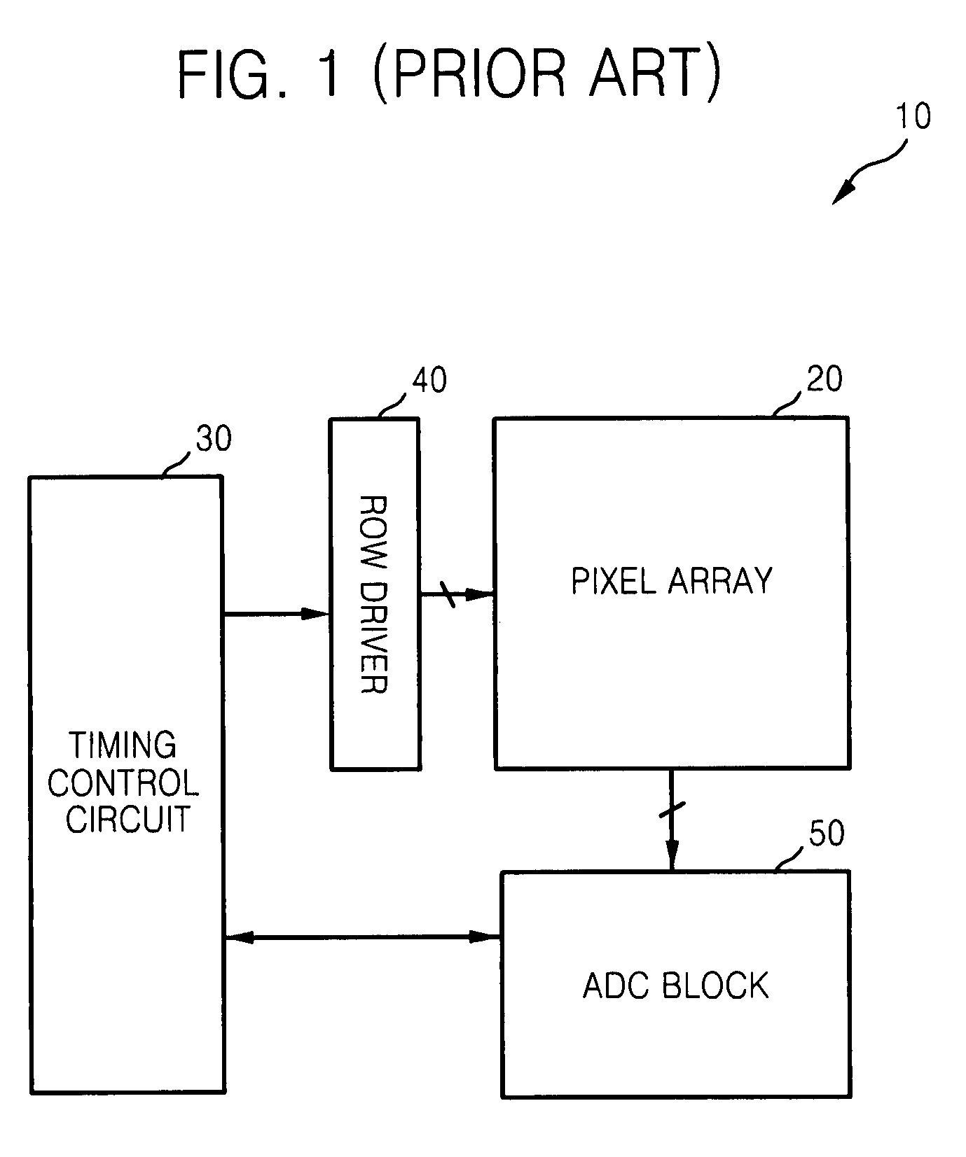
[0048]FIG. 8 shows an image sensor 800 including the CDS and ADC apparatus 400. The image sensor 800 includes a timing control circuit 802, a row driver 804, a pixel array 806, and an ADC (analog to digital converter) block 808. The row driver 804 selects a row of pixels in the pixel array 806 for generating pixel signals to be processed by the ADC block 808 in response to control signals from the timin...


PUM


Abstract

For analog to digital conversion with correlated double sampling in an image sensor, a pixel signal from a given pixel is sampled to generate a respective sampled signal N-times, with N>1 within a horizontal scan time period. A ramp signal is generated with a respective ramping portion for each respective sampled signal. Each respective sampled signal is compared with a respective ramping portion to generate a respective comparison signal that determines a respective digital code. The N respective digital codes are summed to generate a final digital code with reduced random noise.

Description

BACKGROUND OF THE INVENTION [0001] This application claims priority under 35 USC §119 to Korean Patent Application No. 2006-86688, filed on Sep. 8, 2006 in the Korean Intellectual Property Office, the disclosure of which is incorporated herein in its entirety by reference. [0002] 1. Field of the Invention [0003] The present invention relates generally to image sensors such as CMOS (complementary metal oxide semiconductor) image sensors, and more particularly, to using multiple samplings of a reset signal and an image signal from a pixel during a horizontal scan time period for ADC (analog to digital conversion) with CDS (correlated double sampling) to reduce random noise. [0004] 2. Background of the Invention [0005] An image sensor captures an image from photo-conversion of light by a semiconductor material. Charge coupled devices (CCD) are such an example of an image sensor. More recently, CMOS (complementary metal oxide semiconductor) image sensors using CMOS transistors have been...

Claims


Application Information

Patent Timeline
Patent Type & Authority Applications(United States)
IPC IPC(8): H04N5/335H03M1/08H03M1/56H04N5/341H04N5/357H04N5/363H04N5/374H04N5/378
CPCH04N5/378H04N5/3575H04N25/616H04N25/75H04N25/76
Inventor LEE, MYOUNG-SUHAN, JUNE-SOO
Owner SAMSUNG ELECTRONICS CO LTD
Why Eureka
Try Eureka