Embedded capacitors for reducing package cracking

a technology of embedded capacitors and cracking, applied in the field of microelectronics, can solve the problems of increasing the need for decoupling capacitors near the die, reducing the number and size of surface mounted capacitors that can be placed near the die, and causing stress at the interface of materials

Inactive Publication Date: 2008-04-24
INTEL CORP
View PDF4 Cites 19 Cited by
  • Summary
  • Abstract
  • Description
  • Claims
  • Application Information

AI Technical Summary

Problems solved by technology

As increasingly complex microelectronic dies consume more power, the need for decoupling capacitors near the die also increases.
The number and size of surface mounted capacitors that can be placed near the die is limited by the footprint of the capacitors and space available on the mounting substrate.
The CTE mismatch between two or more materials, such as between a microelectronic die and a mounting substrate, induces stress at the interface of the materials during manufacture and operation.
Consequently, the C4 joints are stressed and often crack.
This problem is exacerbated by large dies and thick, stiff substrates, such as those used in high end servers.
This solution is not ideal because of the high cost of ceramic substrates.
This alternative, however, reduces the total amount of power and input / output (I / O) available under the die.
Likewise, increasing the pitch between C4 joints reduces the amount of power and I / O available to a chip.

Method used


Image

  • Embedded capacitors for reducing package cracking
  • Embedded capacitors for reducing package cracking
  • Embedded capacitors for reducing package cracking

Examples


Embodiment Construction

[0027]In various embodiments, an apparatus and method relating to the formation and structure of a mounting substrate for a microelectronic die are described. However, one skilled in the relevant art will recognize that the various embodiments may be practiced without one or more of the specific details. Well-known structures, materials, or operations are not described in detail to avoid unnecessarily obscuring the present invention. Further, various embodiments shown in the figures are illustrative representations and are not necessarily drawn to scale.

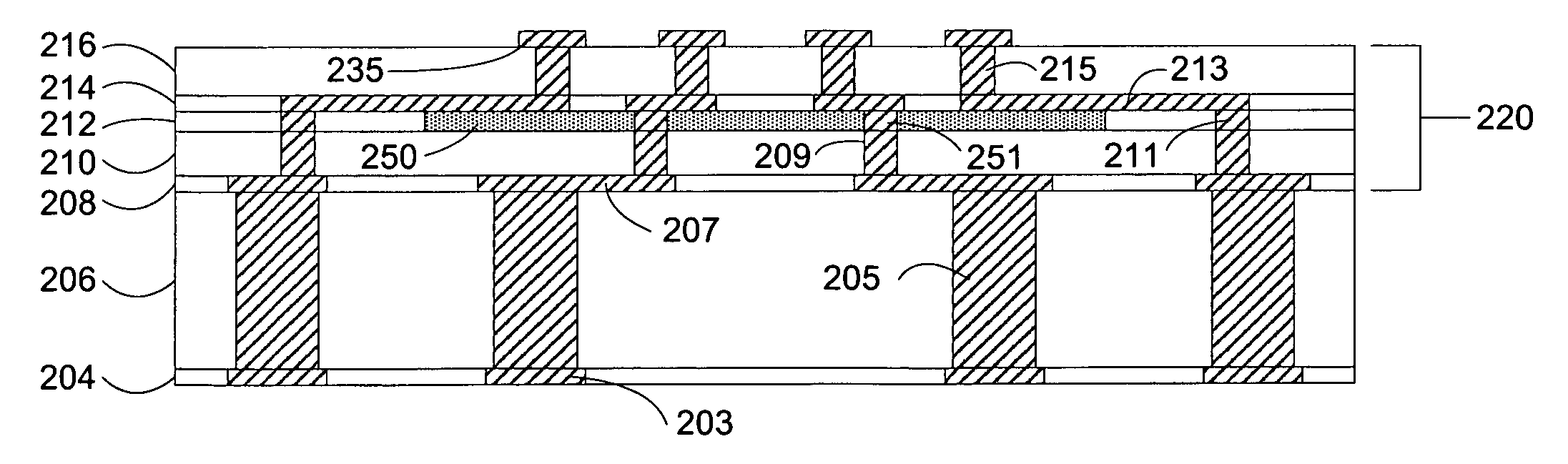
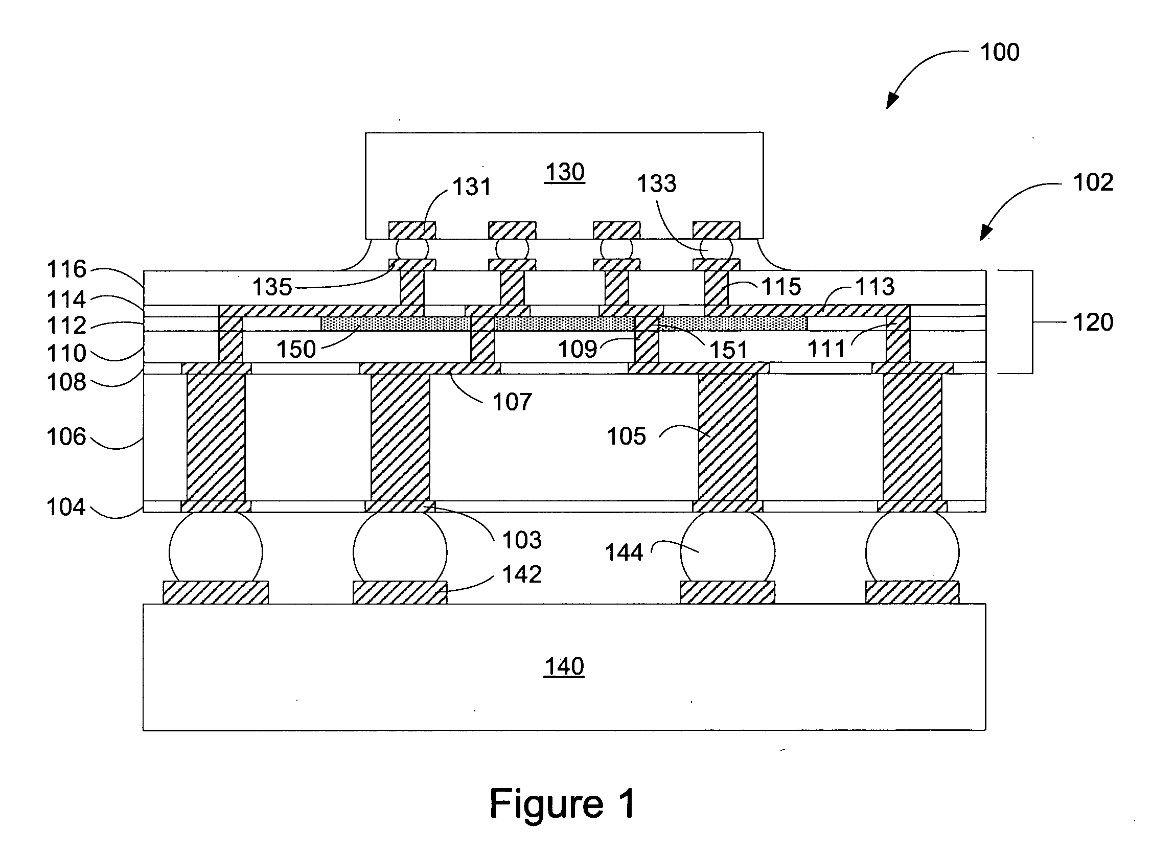
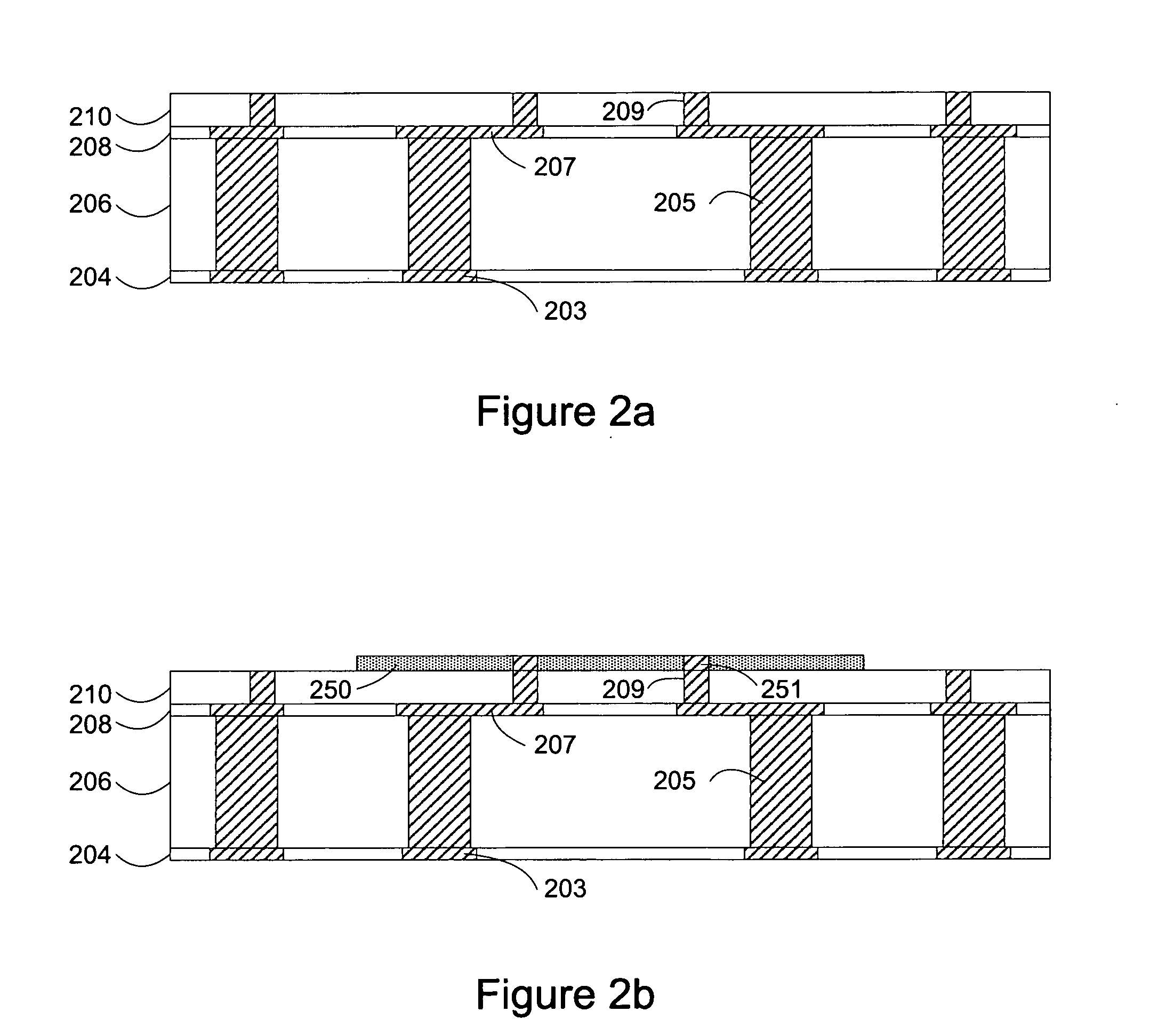
[0028]FIG. 1 illustrates a device 100 including a microelectronic die 130, a mounting substrate 102 connected to the die 130, and a printed circuit board 140 connected to the mounting substrate 102. The die 130 comprises a silicon substrate which has a CTE of approximately 3 ppm / K°. Alternatively, the die 130 may be formed of other materials such as SiGe. The die 130 includes electrical contacts 131 which have a “pitch,” the distance...


PUM


Abstract

A linear coefficient of thermal expansion (CTE) mismatch between two materials, such as between a microelectronic die and a mounting substrate, may induce stress at the interface of the materials. The temperature changes present during the process of attaching a die to a mounting substrate can cause cracking and failure in the electrical connections used to connect the die and mounting substrate. A material with a CTE approximately matching the die CTE is introduced in the mounting substrate to reduce the stress and cracking at the electrical connections between the die and mounting substrate. Additionally, this material may comprise thin film capacitors useful for decoupling power supplies.

Description

FIELD OF INVENTION[0001]The invention relates to the field of microelectronics, and more particularly to the packaging of microelectronics.PRIOR AND RELATED ART[0002]To make a system with an integrated circuit, such as a microprocessor, a microelectronic die is often bonded to a mounting substrate. The mounting substrate may be coupled to another component such as a printed circuit board. Electrical contacts on the die may be connected to corresponding contacts on the side of the mounting substrate facing the die.[0003]As increasingly complex microelectronic dies consume more power, the need for decoupling capacitors near the die also increases. Accordingly, decoupling capacitors are often mounted close to the die on the same mounting substrate surface to which the die is attached. The number and size of surface mounted capacitors that can be placed near the die is limited by the footprint of the capacitors and space available on the mounting substrate.[0004]Materials used to constr...

Claims


Application Information

Patent Timeline
Patent Type & Authority Applications(United States)
IPC IPC(8): H01L21/00H01L23/02
CPCH01L23/15H01L2924/09701H01L2924/01322H01L2924/15311H01L2224/73204H01L2224/32225H01L2224/16225H01L23/147H05K2201/10674H05K2201/068H05K2201/0179H05K2201/0175H05K1/0271H05K1/162H05K3/4644H01L2924/00H01L2224/05567H01L2224/05573H01L2924/00014H01L2224/0554H01L2224/05599H01L2224/0555H01L2224/0556
Inventor MODI, MITULRANGARAJ, SUDARSHAN V.GANAPATHYSUBRAMANIAN, SHANKARHARRIES, RICHARD J.SUBRAMANIAN, SANKARA J.
Owner INTEL CORP
Why Eureka
Try Eureka