Phase change memory devices having dual lower electrodes and methods of fabricating the same

a memory device and lower electrode technology, applied in the field of semiconductor devices, can solve the problems of consuming a small amount of power, affecting the efficiency of phase change, and deteriorating characteristics of the gst layer, and achieve the effect of optimizing phase change efficiency

Active Publication Date: 2008-05-01
SAMSUNG ELECTRONICS CO LTD
View PDF7 Cites 103 Cited by
  • Summary
  • Abstract
  • Description
  • Claims
  • Application Information

AI Technical Summary

Benefits of technology

[0012]Embodiments exemplarily described herein can provide a semiconductor device such as a memory device having dual lower electrodes suitable for optimizing phase change efficiency. Other embodiments exemplarily described herein provide methods of fabricating such semiconductor devices.

Problems solved by technology

As a result, characteristics of the GST layer may deteriorate.
In this case, there is a problem that an ohmic contact is not be formed between the titanium nitride layer forming the lower electrode 20, and the metal silicide layer 28 forming the diode electrode, particularly, between the titanium nitride layer and a cobalt silicide layer.
In addition, semiconductor device are generally required to be fabricated with a high integrity and consume a low amount of power.
The increased resistance of the heater has a disadvantage of reducing a sensing margin of the phase change memory cell.

Method used


Image

  • Phase change memory devices having dual lower electrodes and methods of fabricating the same
  • Phase change memory devices having dual lower electrodes and methods of fabricating the same
  • Phase change memory devices having dual lower electrodes and methods of fabricating the same

Examples


Embodiment Construction

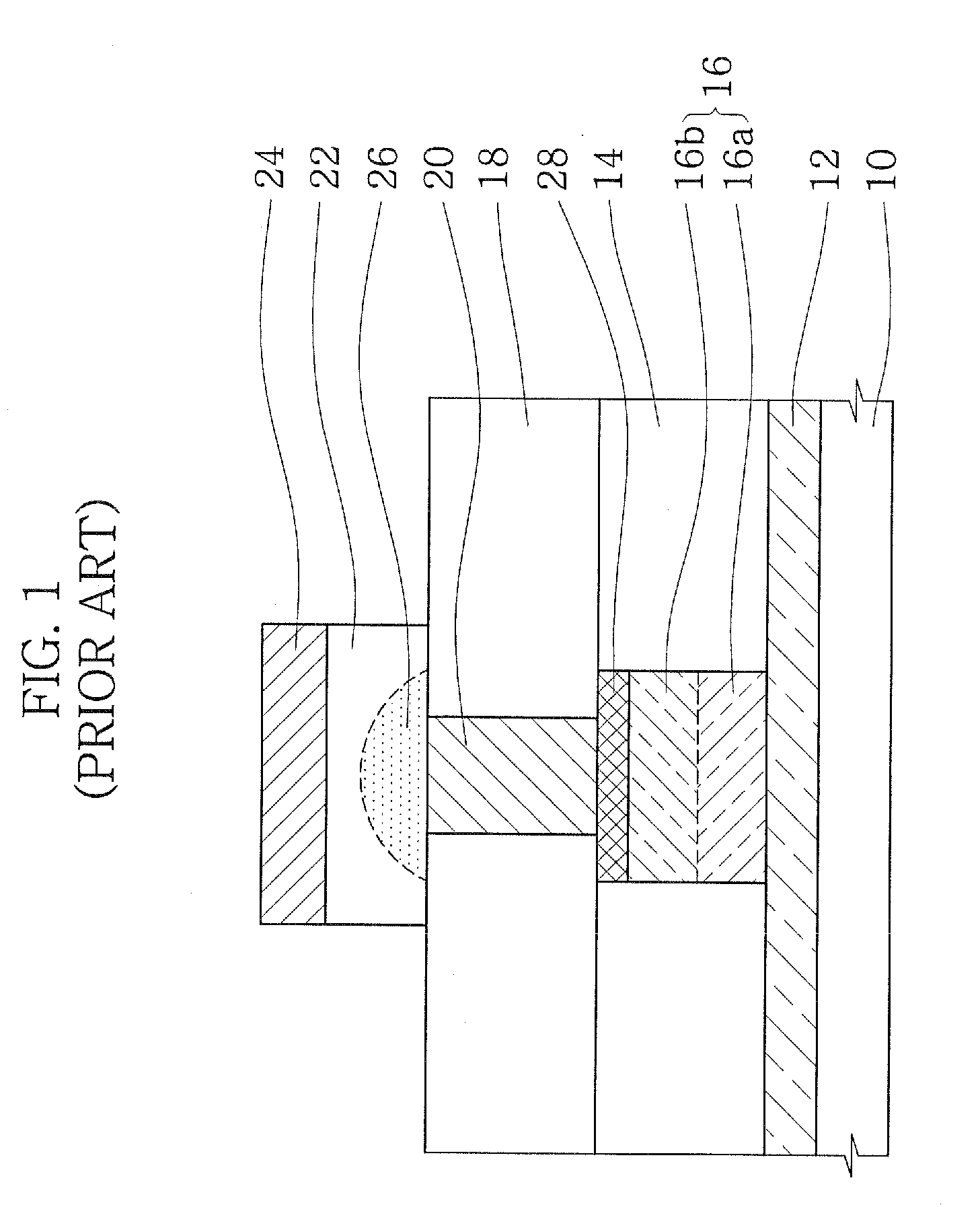
[0023]Exemplary embodiments of the present invention will now be described more fully hereinafter with reference to the accompanying drawings. These embodiments may, however, be realized in different forms and should not be construed as limited to the embodiments set forth herein. Rather, these embodiments are provided so that this disclosure is thorough and complete and fully conveys the scope of the invention to those skilled in the art. In the drawings, the thicknesses of layers and regions are exaggerated for clarity. The same reference numerals are used to denote the same elements throughout the specification. In addition, when a layer is described to be formed on other layer or on a substrate, which means that the layer may be formed on the other layer or on the substrate, or a third layer may be interposed between the layer and the other layer or the substrate.

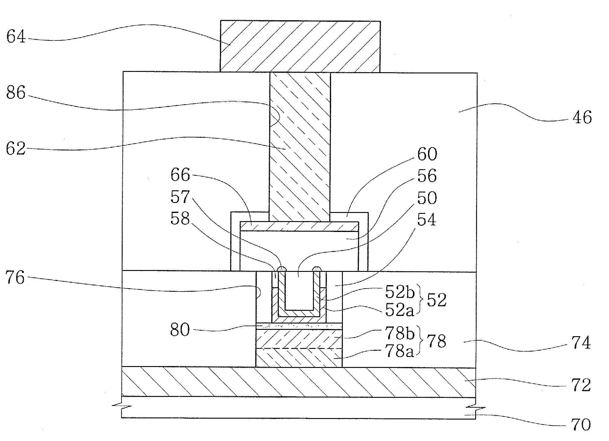
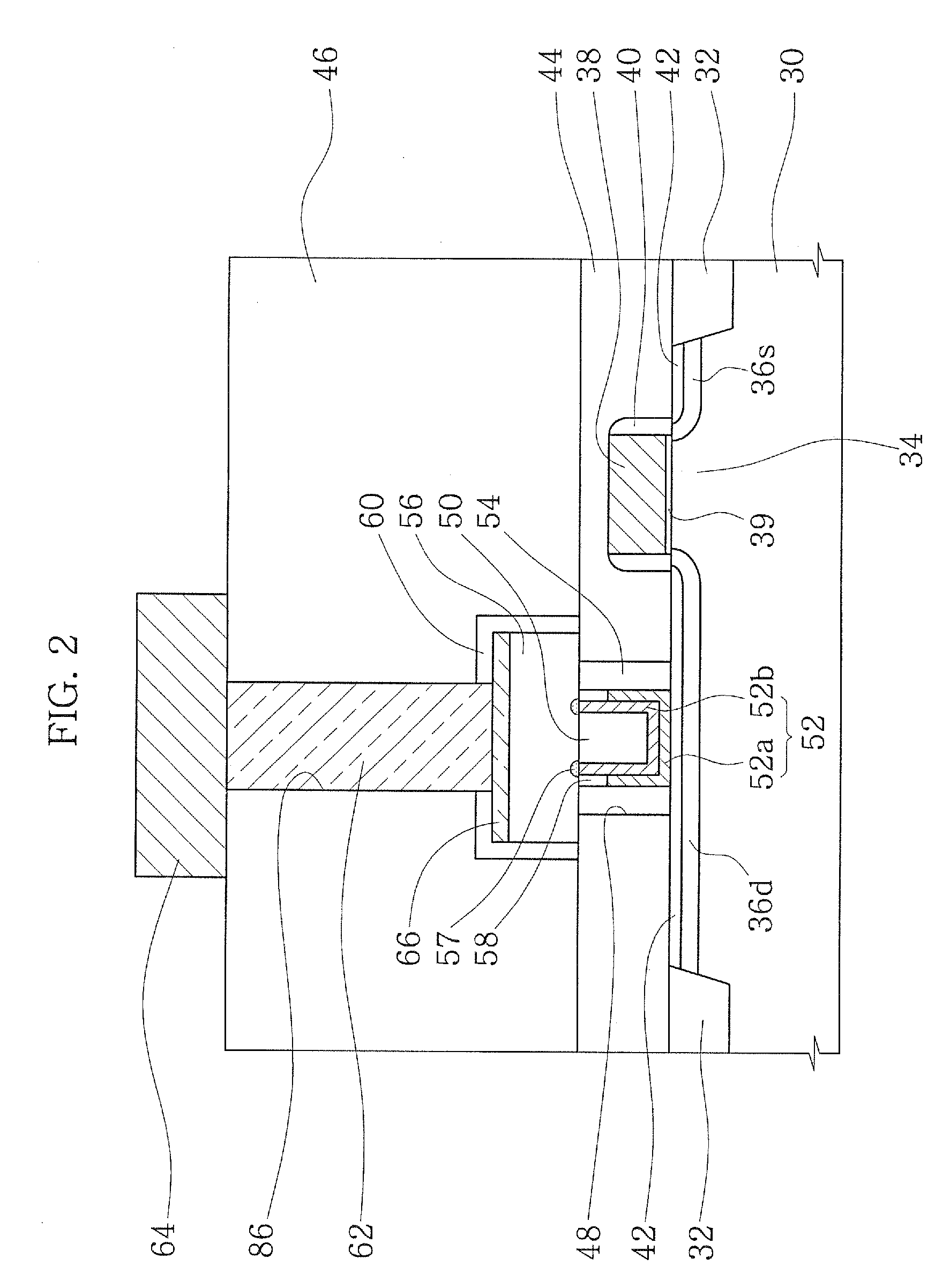
[0024]FIG. 2 is a cross-sectional view of a phase change memory device according to one exemplary embodiment. FIG. 3 ...


PUM


Abstract

A semiconductor device includes a semiconductor substrate and a lower interlayer insulating layer disposed on the substrate. An opening passing through the lower interlayer insulating layer and exposing the substrate is included. A buried insulating pattern is disposed in the opening. First and second conductive layer patterns are sequentially stacked to surround the sidewall and bottom of the buried insulating pattern. A phase change material pattern is included, which is disposed on the lower interlayer insulating layer in contact with a top surface of the second conductive layer pattern, and spaced apart from the first conductive layer pattern. An upper interlayer insulating layer covering the lower interlayer insulating layer and the phase change material pattern is included. A conductive plug is included, which passes through the upper interlayer insulating layer and is electrically connected to the phase change material pattern. A method of fabricating the semiconductor device is also provided.

Description

CROSS-REFERENCE TO RELATED APPLICATION[0001]This application claims the benefit of foreign priority to Korean Patent Application No. 2006-106532, filed Oct. 31, 2006, the contents of which are hereby incorporated herein by reference in their entirety.BACKGROUND[0002]1. Field of Invention[0003]Embodiments of the present invention relate generally to semiconductor devices and methods of fabricating the same. More particularly embodiments of the present invention relate to phase change memory devices having dual lower electrodes, and methods of fabricating the same.[0004]2. Description of Related Art[0005]Recently, a phase change memory device has been proposed as a novel semiconductor device. Phase change memory devices have a nonvolatile characteristic, and thus do not lose data stored therein even if power is interrupted. A unit cell of the phase change memory device includes a switching device and a data storage element serially connected to the switching device. The data storage e...

Claims


Application Information

Patent Timeline
Patent Type & Authority Applications(United States)
IPC IPC(8): H01L47/00H01L21/00
CPCH10B63/20H10B63/30H10N70/8413H10N70/8418H10N70/231H10N70/8828H10N70/063H10N70/826G11C13/0004
Inventor SONG, YOON-JONGRYOO, KYUNG-CHANGLIM, DONG-WON
Owner SAMSUNG ELECTRONICS CO LTD
Why Eureka
Try Eureka