One transistor dram cell structure and method for forming

a dram cell and transistor technology, applied in semiconductor devices, digital storage, instruments, etc., can solve the problems of too slow erase, too slow write, and insufficient speed of writing and erasing

Active Publication Date: 2008-05-01
NXP USA INC
View PDF11 Cites 104 Cited by
  • Summary
  • Abstract
  • Description
  • Claims
  • Application Information

AI Technical Summary

Problems solved by technology

One of the difficulties has been in achieving both writing and erasing with sufficient speed.
If the hole removal is not sufficiently faster than hole/electron pair generation in the erase mode, then the erase is ...

Method used


Image

  • One transistor dram cell structure and method for forming
  • One transistor dram cell structure and method for forming
  • One transistor dram cell structure and method for forming

Examples


Embodiment Construction

[0011]For a thorough understanding of the subject One Transistor DRAM Cell Structure and Method for Forming, reference is made to the following Detailed Description, which includes the appended Claims, in conjunction with the above-described Drawings.

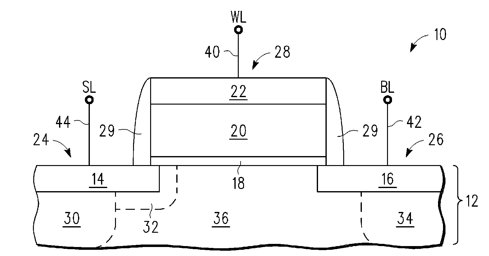
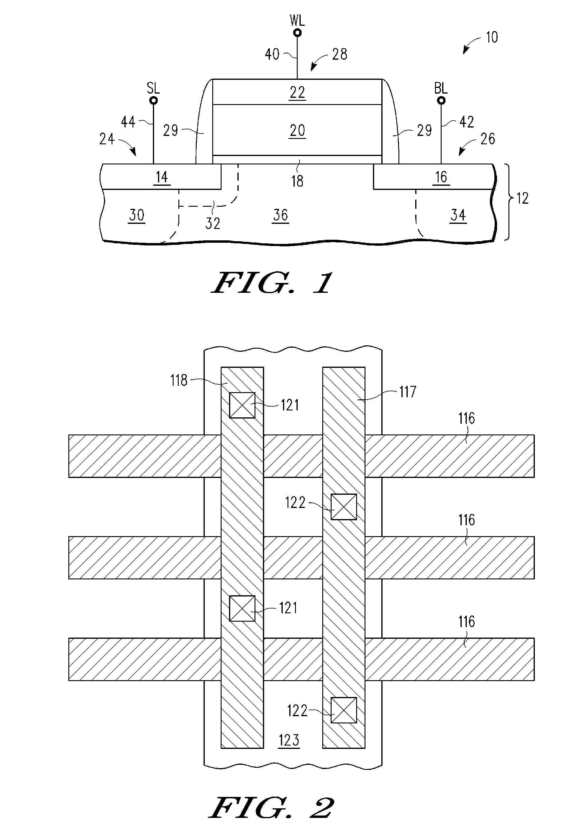
[0012]In a manner that will become eminently apparent below, the subject invention inheres, in one form, in a structure and method for programming a single-transistor capacitorless (1T / 0C) memory cell. Specifically, the memory cell, which comprises a floating (i.e., isolated) body region, is programmed by modulating the threshold voltage, VT, of a MOS transistor that includes the body region and respective drain and source regions. VT modulation is effected through the accumulation, as a result of band-to-band tunneling (BTBT), of majority carriers in the body region. Programming the memory cell in this manner is preferable to other known techniques in that, inter alia, generation of majority carriers by BTBT demands appreciably lower...


PUM


Abstract

A one-transistor dynamic random access memory (DRAM) cell includes a transistor which has a first source/drain region, a second source/drain region, a body region between the first and second source/drain regions, and a gate over the body region. The first source/drain region includes a Schottky diode junction with the body region and the second source/drain region includes an n-p diode junction with the body region.

Description

FIELD OF THE INVENTION [0001]The invention relates in general to semiconductor devices, and in particular to a DRAM cell having one transistor.RELATED ART[0002]DRAMs (dynamic random access memories) in general have enjoyed great success primarily due to the high density with good speed. In the quest for even higher density, a technique for single transistor DRAMs has been developed. The individual cell is provided in a semiconductor on insulator (SOI) substrate or on a bulk substrate with isolated transistor bodies and requires only a single transistor, doing away with the need for the capacitor that has historically been used in DRAMs. These types of DRAM cells are also known as capacitorless DRAM cells because of not requiring a capacitor. In such a single transistor DRAM cell, the body of the transistor is left floating and, because the bodies of the transistors are isolated from each other, charge is accumulated in the body. This alters the threshold of the transistor, and such ...

Claims


Application Information

Patent Timeline
IPC IPC(8): H01L29/94
CPCG11C11/404G11C2211/4016H01L27/0207H01L29/7841H01L27/10802H01L27/10844H01L29/7839H01L27/108H10B12/20H10B12/01H10B12/00H01L29/41725
Inventor BURNETT, JAMES D.WINSTEAD, BRIAN A.
Owner NXP USA INC
Why Eureka
Try Eureka