Signal detecting circuit
a signal detection and circuit technology, applied in the field of signal detection circuits, can solve the problems of increasing manufacturing steps, increasing costs, and being unable to accurately detect the received signal, and achieve the effect of accurately detecting presence and absen
- Summary
- Abstract
- Description
- Claims
- Application Information
AI Technical Summary
Benefits of technology
Problems solved by technology
Method used
Image

Examples
first embodiment
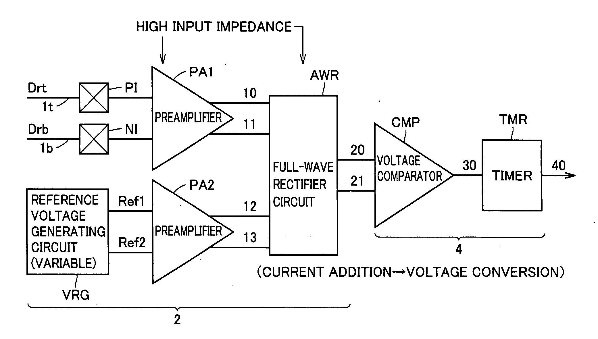
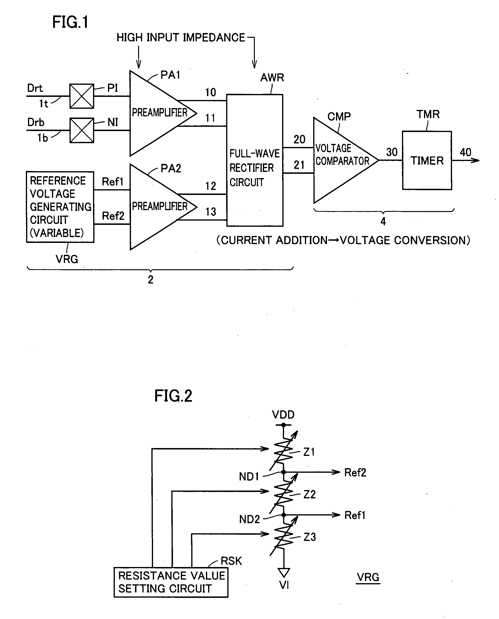
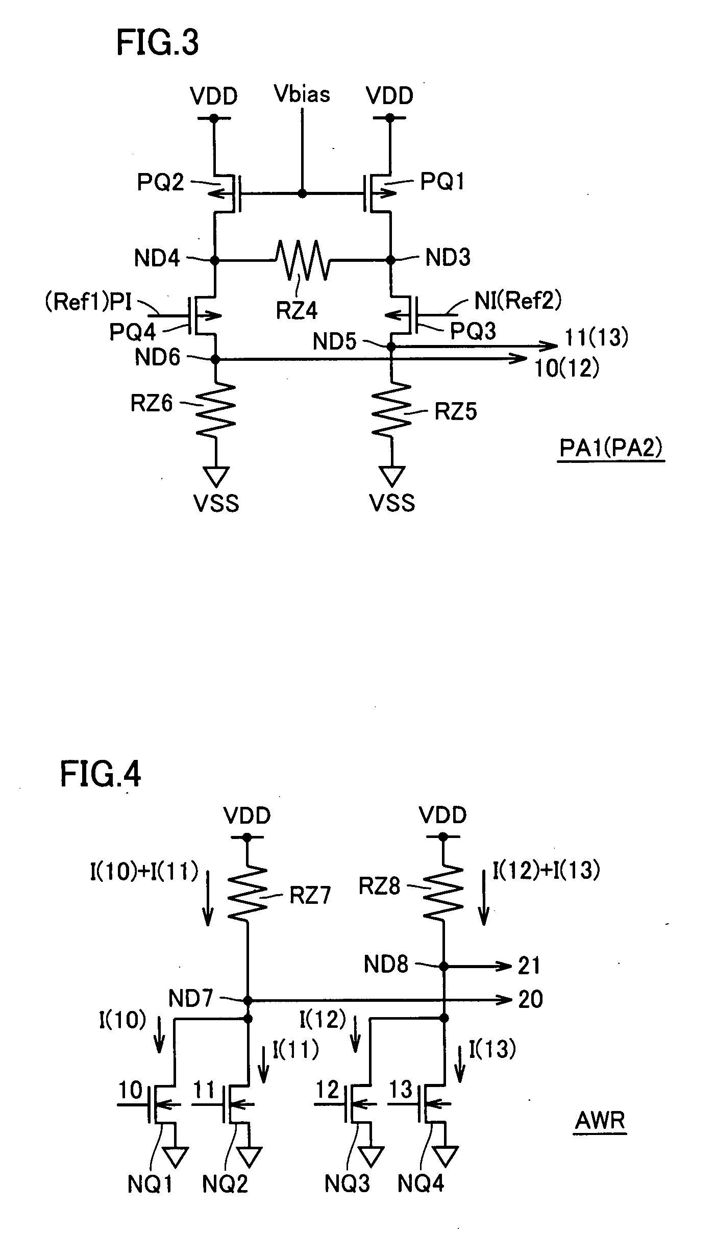
[0044]FIG. 1 schematically shows a whole construction of a signal detecting circuit according to a first embodiment of the invention. In FIG. 1, the signal detecting circuit includes an input circuit 2 produces, according to a difference value of a differential signal formed of complementary signal Drt, Drb transmitted through complementary signals 1t and 1b and a difference value between reference voltages Ref1 and Ref2, signals 20 and 21 indicating magnitudes of these difference values, and an internal signal producing circuit 4 that produces a signal 40 indicating a logical level of differential signal Drt, Drb according to complementary output signals 20 and 21 of input circuit 2.
[0045] In signal transmission, differential signal Drt, Drb is formed of complementary signals that change toward higher and lower sides by substantially the same amplitude ΔV with a reference voltage (a common level) being a center. Accordingly, the amplitude of differential signal Drt, Drb is given b...
second embodiment
[0112]FIG. 10 schematically shows a whole construction of a signal detecting circuit according to a second embodiment of the invention. The signal detecting circuit shown in FIG. 10 differs from that in FIG. 1 in the following configurations. In input circuit 2, a current mirror type full-wave rectifier circuit CAWR is employed for full-wave rectifier circuit AWR. In the current mirror type full-wave rectifier circuit CAWR, differential amplification is performed by a current mirror operation according to the added value of output signals 10 and 11 of preamplifier PA1 and the added value of output signals 12 and 13 of preamplifier PA2, and complementary output signals 20 and 21 are produced.
[0113] Other configurations of the signal detecting circuit shown in FIG. 10 are the same as those of the signal detecting circuit shown in FIG. 1. The corresponding components are allotted the same reference numerals, and description thereof will not be repeated.
[0114]FIG. 11 shows an example ...
third embodiment
[0136]FIG. 13 schematically shows a whole construction of a signal detecting circuit according to a third embodiment of the invention. The signal detecting circuit shown in FIG. 13 differs from the signal detecting circuit shown in FIG. 1 in the following configurations. In input circuit 2, the voltages V1 and V2 applied to preamplifier PA2 are at fixed voltage levels. The full-wave rectifier circuit receiving output signals 10-13 of preamplifiers PA1 and PA2 is formed of an output-amplitude-variable full-wave rectifier circuit VAWR. Output-amplitude-variable full-wave rectifier circuit VAWR adjusts the comparison reference amplitude, to adjust the detection threshold of the amplitude of differential signal Drt, Drb.
[0137]FIG. 14 shows an example of the construction of output-amplitude-variable full-wave rectifier circuit VAWR shown in FIG. 13. Output-amplitude-variable full-wave rectifier circuit VAWR shown in FIG. 14 differs from full-wave rectifier circuit AWR shown in FIG. 1 in...
PUM
 Abstract
Description
Claims
Application Information
 - R&D
- Intellectual Property
- Life Sciences
- Materials
- Tech Scout
- Unparalleled Data Quality
- Higher Quality Content
- 60% Fewer Hallucinations
Browse by: Latest US Patents, China's latest patents, Technical Efficacy Thesaurus, Application Domain, Technology Topic, Popular Technical Reports.
© 2025 PatSnap. All rights reserved.Legal|Privacy policy|Modern Slavery Act Transparency Statement|Sitemap|About US| Contact US: help@patsnap.com