Method of forming an isolation layer and method of manufacturing an image device using the same

a technology of isolation layer and manufacturing method, which is applied in the manufacturing of semiconductor/solid-state devices, semiconductor devices, electrical devices, etc., can solve the problems of difficult integration of signal processing units in ccd chips, high power consumption and fabrication process, and complicated driving operation of ccd image devices, so as to prevent or reduce the likelihood of electron infiltrating into an active region

Inactive Publication Date: 2008-05-01
SAMSUNG ELECTRONICS CO LTD
View PDF8 Cites 37 Cited by
  • Summary
  • Abstract
  • Description
  • Claims
  • Application Information

AI Technical Summary

Benefits of technology

[0013]It is therefore a feature of an embodiment of the present invention to provide a method of forming an isolation layer that is less susceptible to the generation of a seam or a void in an isolation pattern.
[0014]It is therefore a feature of an embodiment of the present invention to provide a method of forming an isolation layer that prevents or reduces the likelihood that an electron would infiltrate into an active region.

Problems solved by technology

The CCD image device may have a complicated driving operation, a high power consumption and a complicated fabrication process.
Further, since integrating a signal processing unit in a CCD chip may be difficult, forming the CCD image device as a single chip may also be difficult.
Moreover, as trenches become deeper, it becomes more difficult to completely fill the trench with isolation material.
Consequently, a seam or a void in the isolation pattern may result so that the image device may suffer from deteriorated characteristics.

Method used


Image

  • Method of forming an isolation layer and method of manufacturing an image device using the same
  • Method of forming an isolation layer and method of manufacturing an image device using the same
  • Method of forming an isolation layer and method of manufacturing an image device using the same

Examples


Embodiment Construction

[0020]Korean Patent Application No. 10-2006-0105097 filed on Oct. 27, 2006, in the Korean Intellectual Property Office and entitled “Method of Forming an Isolation Layer and Method of Manufacturing an Image Device Using the Same,” is incorporated by reference herein in its entirety.

[0021]The present invention will now be described more fully hereinafter with reference to the accompanying drawings, in which example embodiments of the present invention are illustrated. The present invention may, however, be embodied in many different forms and should not be construed as limited to the example embodiments set forth herein. Rather, these example embodiments are provided so that this disclosure will be thorough and complete, and will fully convey the scope of the present invention to those skilled in the art.

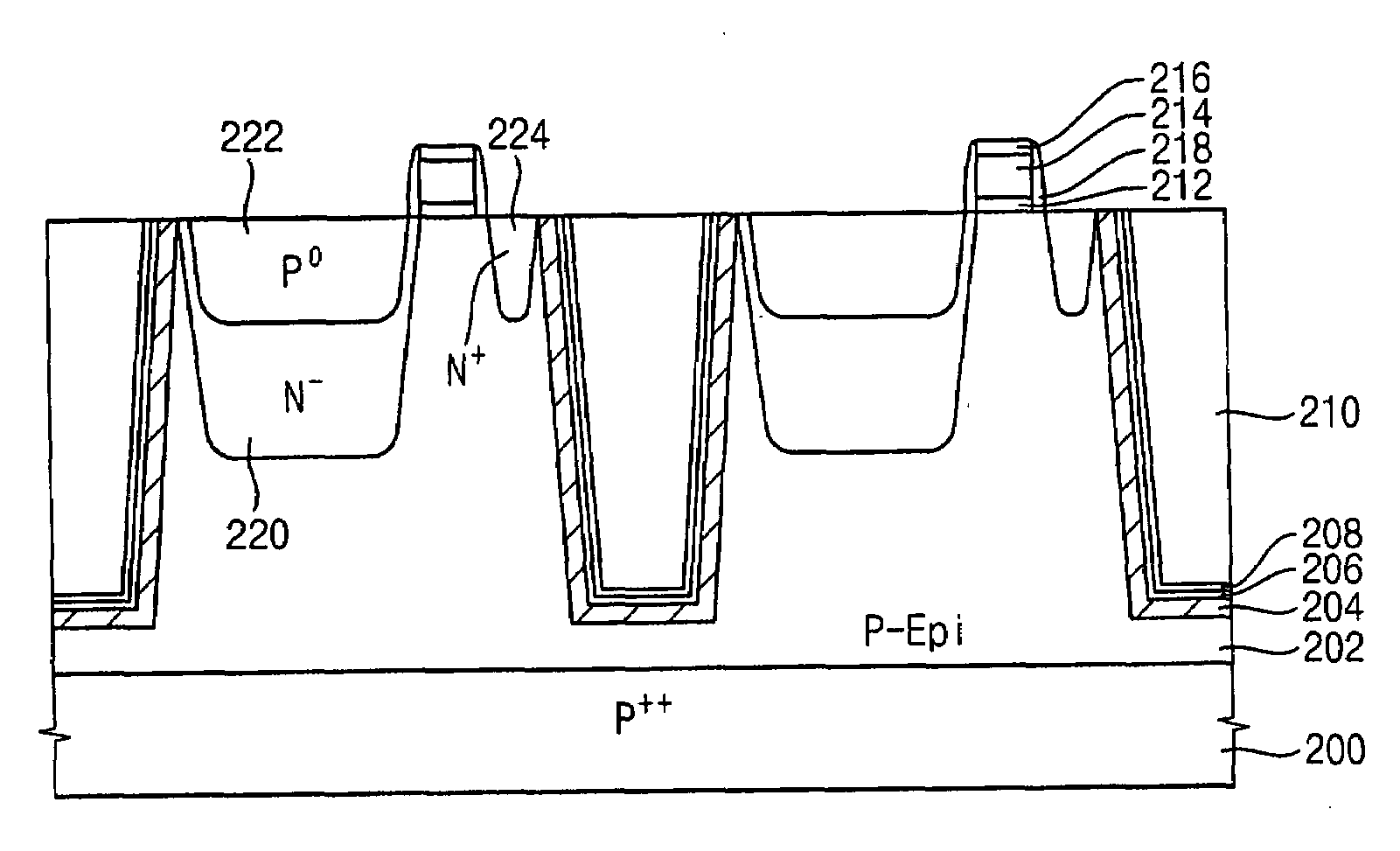
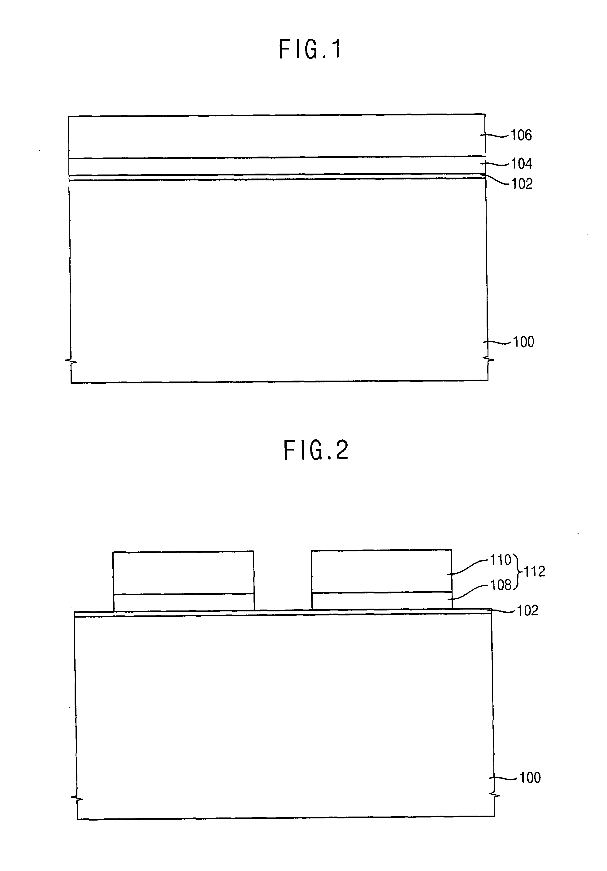
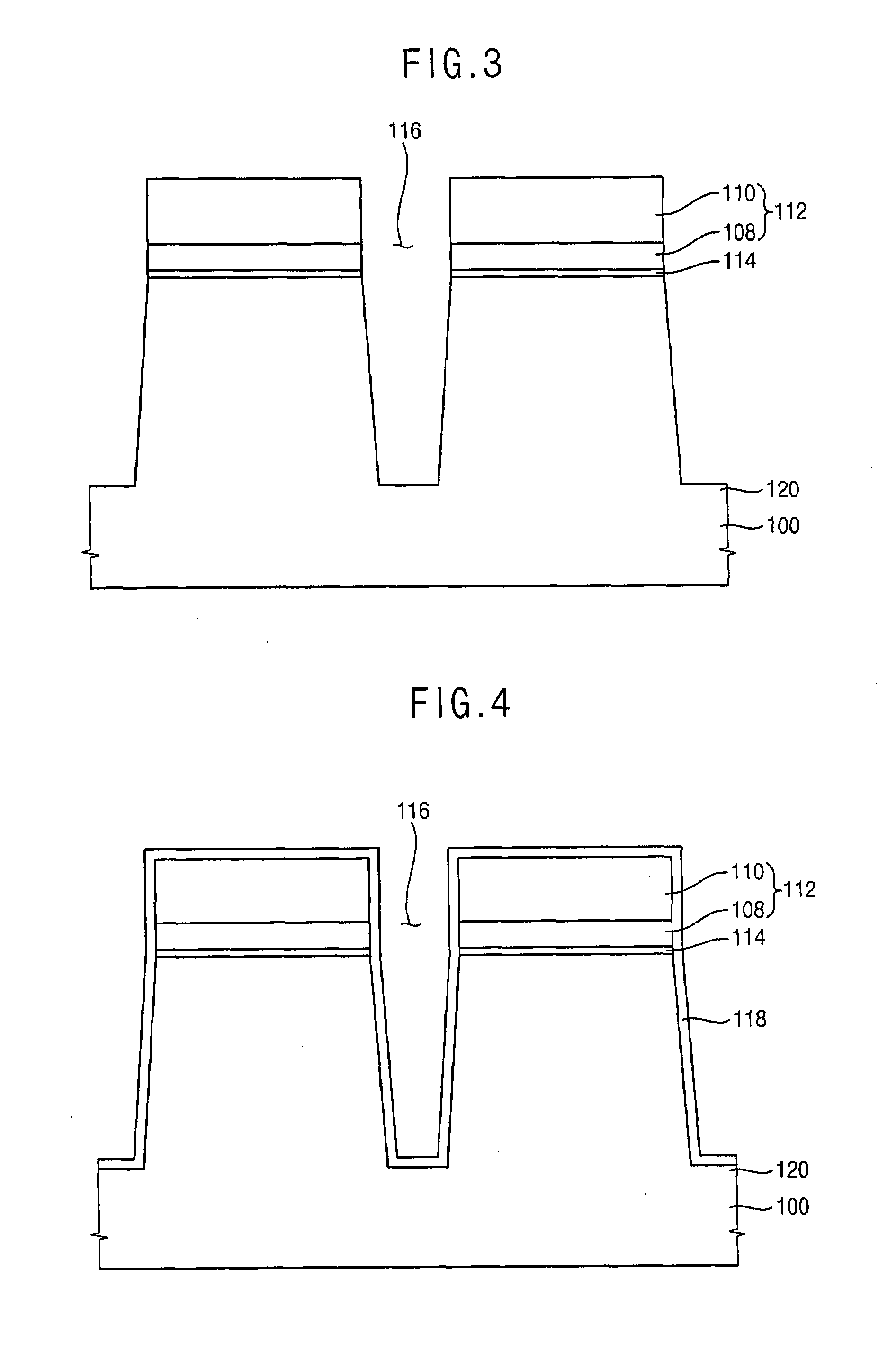
[0022]In the figures, the dimensions of layers and regions may be exaggerated for clarity of illustration. It will also be understood that when a layer or element is referred to as b...


PUM


Abstract

A method of forming an isolation layer includes forming mask pattern structure on a substrate to partially expose the substrate, etching the substrate using the mask pattern as an etching mask to form a trench, forming an impurity diffusion region at an inner face of the trench, and filling the trench with the isolation layer. A method of manufacturing an image device includes the method of forming an isolation layer, and at least additionally forming unit pixels including a photo diode and transistors on an active region defined by the isolation layer.

Description

BACKGROUND OF THE INVENTION[0001]1. Field of the Invention[0002]Example embodiments of the present invention relate to a method of forming an isolation layer and a method of manufacturing an image device using the same.[0003]2. Description of the Related Art[0004]Generally, an image device may correspond to a semiconductor module for converting an optical image into an electrical signal. The image device may be used for storing and transmitting an image signal to a display device for displaying the image signal. The image device may be classified as a charge coupled device (CCD) image device or a complementary metal oxide semiconductor (CMOS) image device.[0005]The CCD image device may include a plurality of MOS capacitors that may be operated by moving charges generated by light. In contrast, the CMOS image device may be driven by a plurality of unit pixels and a CMOS circuit for controlling an output signal of the unit pixels.[0006]The CCD image device may have a complicated drivi...

Claims


Application Information

Patent Timeline
Patent Type & Authority Applications(United States)
IPC IPC(8): H01L31/18H01L21/762
CPCH01L21/76224H01L27/14683H01L27/1463H01L21/76
Inventor KIM, DAE-WOONGLEE, MI-YOUNG
Owner SAMSUNG ELECTRONICS CO LTD
Why Eureka
Try Eureka