
Circuit and method for an SRAM with two phase word line pulse

a technology of word line pulse and circuit, which is applied in the field of circuit and method of sram with two phase word line pulse, can solve the problems of affecting the operating margin of the cell, reducing the manufacturing yield, and affecting the reliability and performance of the sram cell, so as to improve the noise margin reduce or save power consumption, and improve the noise margin effect of the “read” operation

Active Publication Date: 2008-05-08
TAIWAN SEMICON MFG CO LTD
View PDF4 Cites 21 Cited by
  • Summary
  • Abstract
  • Description
  • Claims
  • Application Information

AI Technical Summary

Benefits of technology

[0017]In one preferred embodiment of the circuitry of the invention, a first timing circuit is provided and a second timing circuit is provided, observation circuitry is utilized to monitor the changes in the bit line voltages, and after a predetermined threshold is reached on a falling bit line during an access cycle, a word line suppression circuit is disabled and the word line is allowed to rise from a first voltage that is less than a supply voltage by a delta voltage amount, to an unsuppressed supply voltage level. The suppression circuit on the word line may also be activated during power down cycles to reduce or save power consumption. The timing and access circuitry provided in the preferred embodiments of the present invention circumvent the need for added sense amplifiers or other circuitry as used in the prior art approaches, thus the area penalty for the improved performance of the SRAM incorporating the features of the present invention is minimal and is better than the area penalty associated with the known prior art solutions.
[0018]In a first preferred embodiment, a word line suppression circuit element is provided coupled to each word line. In one embodiment this element may be a MOS transistor, in another alternative preferred embodiment; this element may be a diode or other controlled suppression circuit. A first timing circuit is provided that outputs first word line controls signal. A second timing circuit is provided that outputs second word line controls signal. The word line suppression circuit is normally “on.” The word line pulse is divided into two phases, during the first phase, the first timing circuit provides the first word line control signal and the second timing circuit provides the second word line control signal. During the first phase, the word line decoders are enabled and the bit line voltages are monitored by the first timing circuit. During the first phase, a word line suppression circuit is active and the word line is allowed to rise to a voltage that is a delta voltage or dV less than the supply voltage Vdd. In this manner, when the bit lines are at a high voltage at the beginning of the cycle, the word lines are suppressed to a lower voltage, thus improving the noise margins for a “read” operation.
[0019]When the falling bit line is detected discharging past a predetermined threshold in response to the word line being activated, the first timing circuit stops outputting the first word line control signal and the second phase begins. During the second phase, the second timing circuit continues outputting the second word line control signal until the falling bit line discharges past a second predetermined voltage. During the second phase, the word line suppression circuit is disabled, and therefore the word line is allowed to increase to a higher, unsuppressed voltage. In this manner the second phase provides a higher word line voltage during the time that the bitlines are at a lower voltage, thus increasing the margins for a “write” operation.
[0020]In a preferred method of operating an SRAM, a two phase word line pulse is provided. A word line suppression circuit coupled to the active word line and enabled by timing circuitry is operated to provide a word line voltage in a first phase of an access cycle that is less than the supply potential by a delta voltage, so that during the first phase of an access cycle the word lines are at a voltage that is less than the starting voltage for the bit lines by a delta voltage. During a second phase of the access cycle, the word line suppression circuit is disabled so that the word line rises to the full supply potential, thus when the bit lines are at a lower voltage, the word line is at a higher voltage, this increases the margins for a “write” cycle.

Problems solved by technology

The variability in the threshold voltages has a negative impact on the reliability and performance of the SRAM cell, and this directly affects the operating margins of the cell, such as static noise margin (SNM).
If this is not done, then many IC devices will fail post manufacture reliability tests, thus the manufacturing yield will fall, and the cost of each integrated circuit that does pass the tests will rise commensurately.
As the scaling of the dimensions of CMOS integrated circuitry gets smaller, certain dominant problematic effects become increasingly dominant.
Providing a variable supply voltage depending on which portion of the operation cycle is being performed is one known prior art approach, however this approach requires a complex supply voltage line and extra control circuitry.
While this short pulse on the word lines has a positive impact on the read cycle operating margins, the paper also describes that this approach actually has a negative impact for sense amplifier margins and for the write margins.
This two pulse word line approach requires additional control circuitry complexity; power consumption is increased, and because the write back for each cycle means that each column requires its own dedicated sense amplifier, area is also greatly increased over more space efficient shared sense amplifier approaches.
The SRAM prior art therefore provides a word line maintained at a single voltage during access cycles, and the noise margin problems of the cells are addressed inefficiently by the prior art.

Method used


Image

  • Circuit and method for an SRAM with two phase word line pulse
  • Circuit and method for an SRAM with two phase word line pulse
  • Circuit and method for an SRAM with two phase word line pulse

Examples


Embodiment Construction

[0032]The making and using of the presently preferred embodiments are discussed in detail below. It should be appreciated, however, that the present invention provides many applicable inventive concepts that can be embodied in a wide variety of specific contexts. The specific embodiments discussed are merely illustrative of specific ways to make and use the invention, and do not limit the scope of the invention.

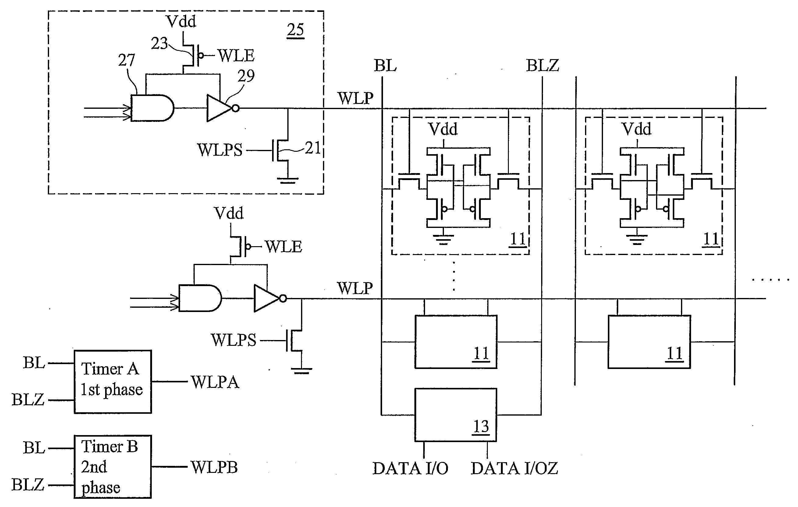
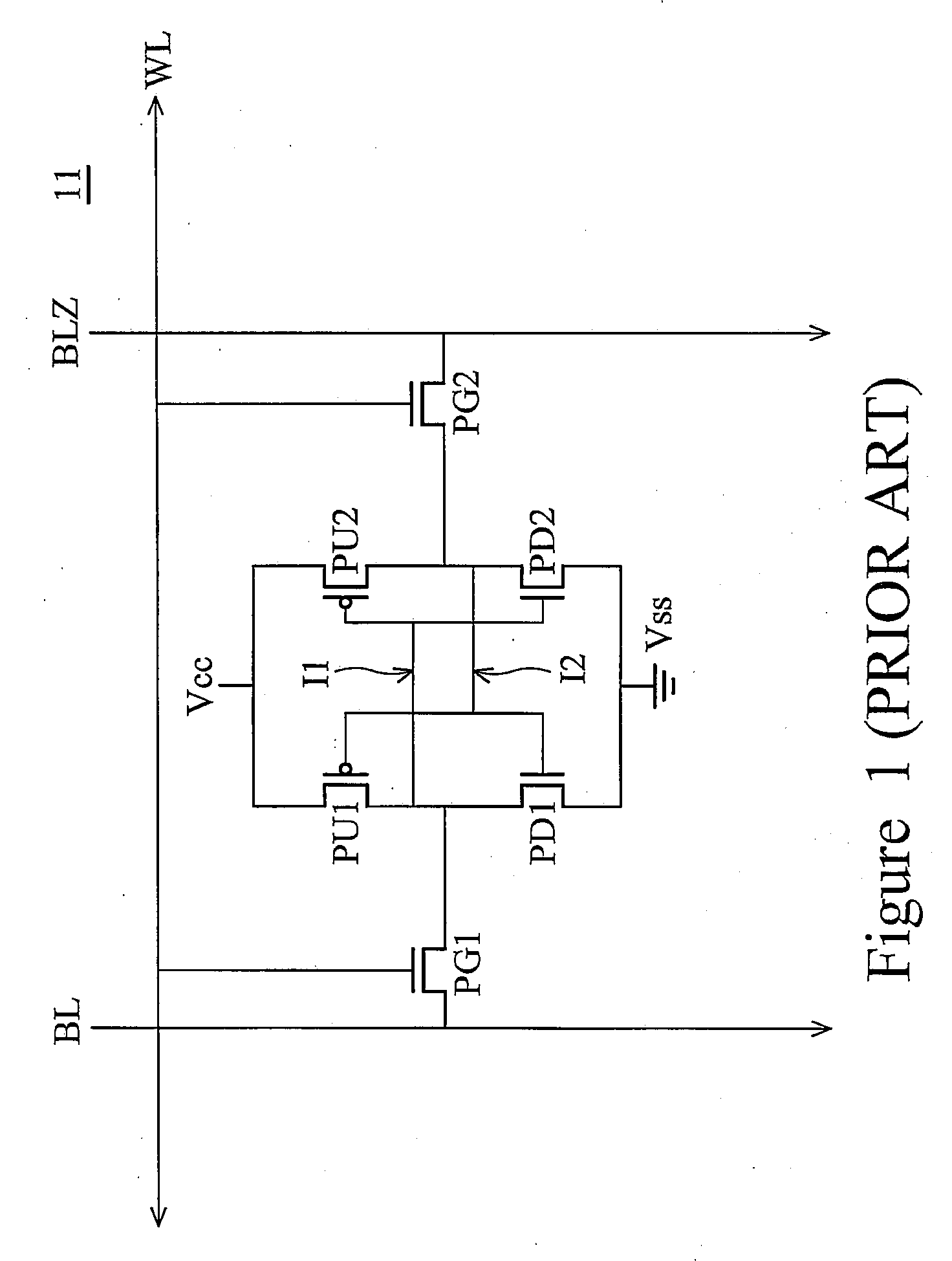
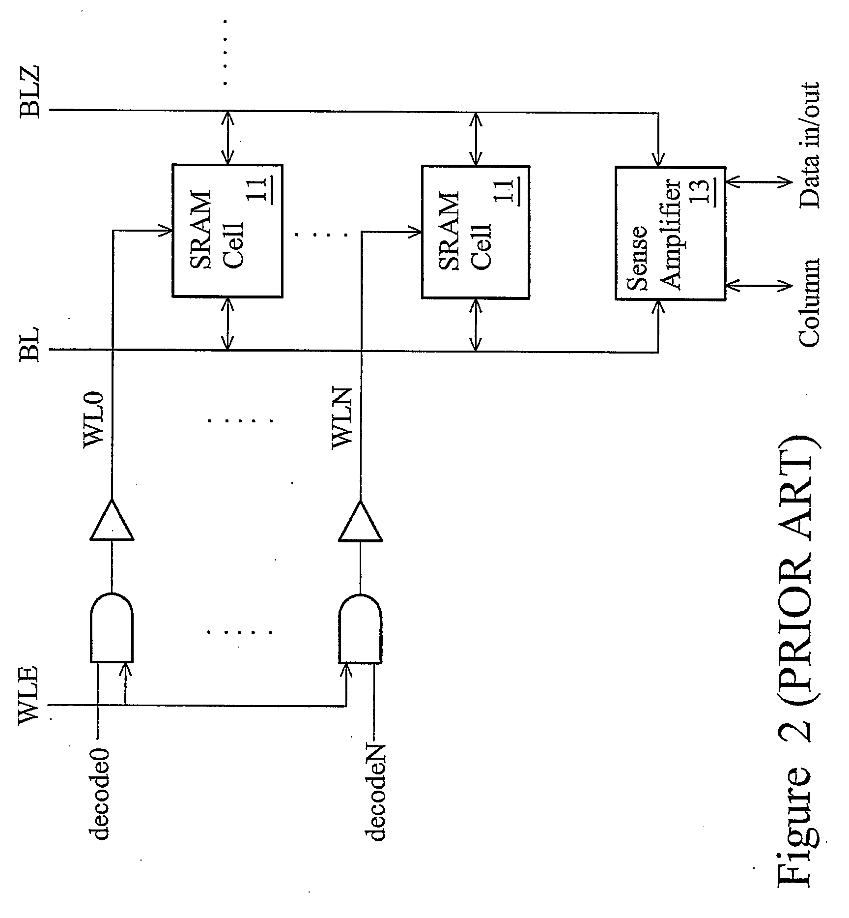
[0033]FIG. 5 depicts in a simple schematic view a first preferred circuit embodiment of the SRAM array incorporating the invention. An array of SRAM cells 11, shown in this exemplary circuit as 6T cells, is arranged in rows and along columns. Typically, each column will be associated with a bit in a data word that is input and output using I / O circuitry (not shown in this view) but other arrangements are also possible. In FIG. 5, the columns are each associated with a pair of column or bit lines that are differential and complementary bit lines, labeled BL and BLZ. As is know...


PUM


Abstract

A circuit and method for providing a two phase word line pulse for use during access cycles in an SRAM memory with improved operating margins. A first and a second timing circuit are provided and a word line voltage suppression circuit is provided to reduce the voltage on the active word lines in a first phase of a word line pulse, and to allow the word lines to rise to a second, unsuppressed voltage in a second phase of the word line pulse, responsive to the first and second timing circuits. The first and second timing circuits observe the bit lines voltage discharge and provide control signals active when the bit lines are discharged past certain thresholds, these signals control the voltage suppression circuit. Operating margins for the SRAM are therefore improved. Methods for operating an SRAM using a two phase word line pulse are provided.

Description

[0001]This application claims the benefit of U.S. Provisional Application No. 60 / 856,423 filed on Nov. 3, 2006, entitled “Two Stage Suppress Pulse Word Line and Negative Bit Line Design,” which application is hereby incorporated herein by reference.TECHNICAL FIELD[0002]The present invention relates to a circuit and method for providing a read circuits, write circuits and a sense amplifier for use in a static RAM (“SRAM”) memory with enhanced margins and performance. The SRAM is manufactured using advanced semiconductor processing technology and small cell size, and the transistors have variable threshold voltages due to the physical characteristics of present advanced semiconductor processes. The circuitry and operation methods of the SRAM are configured to provide improved performance.BACKGROUND[0003]Present and planned semiconductor processes are providing devices for integrated circuits having process minimum feature sizes of 100 nanometers and smaller. Transistors fabricated in ...

Claims


Application Information

Patent Timeline
Patent Type & Authority Applications(United States)
IPC IPC(8): G11C7/02G11C8/00
CPCG11C11/418G11C8/08
Inventor WANG, CHIA WEILEE, CHENG HUNGLIAO, HUNG-JENHSU, FU-CHIEH
Owner TAIWAN SEMICON MFG CO LTD
Learn More