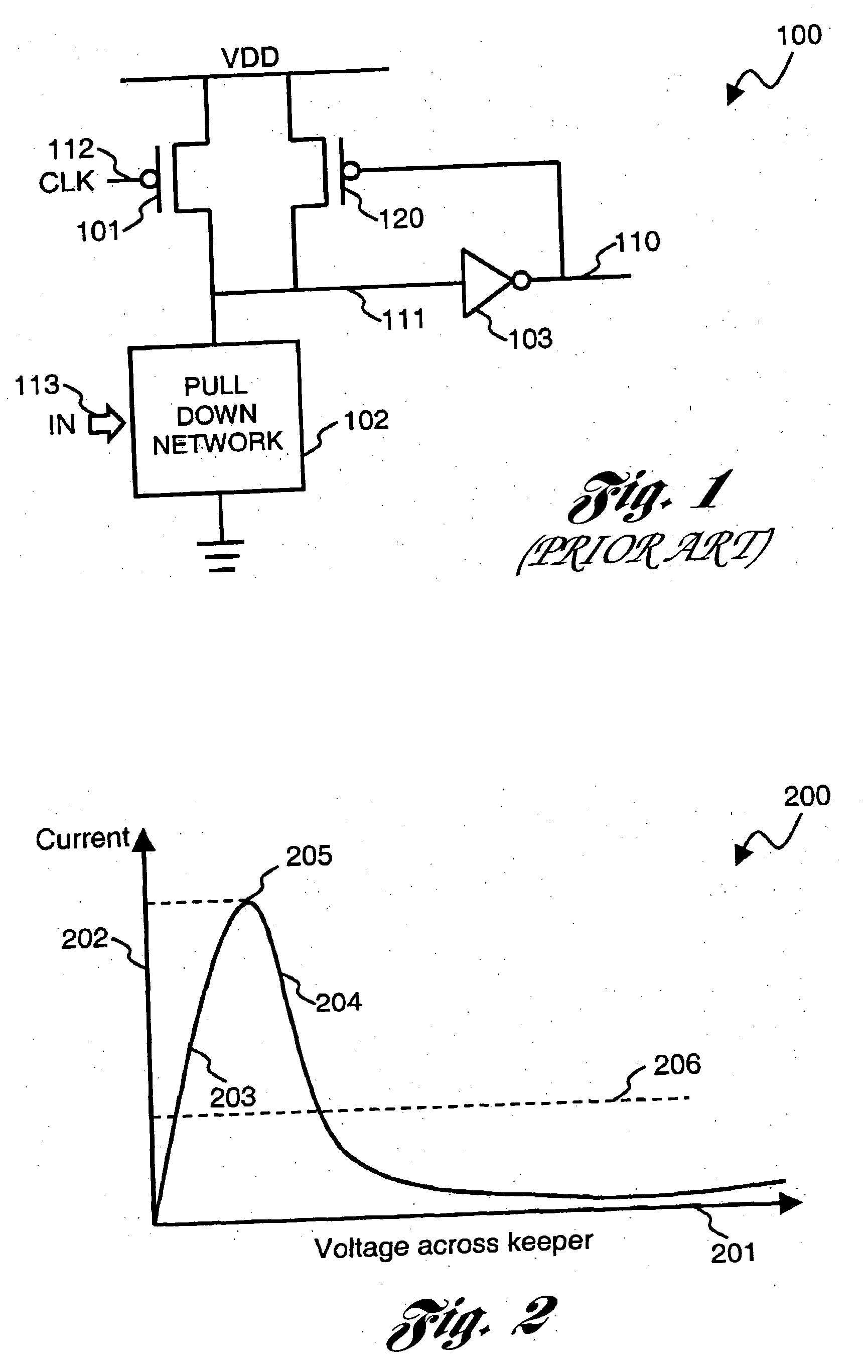
However, dynamic CMOS gates are inherently less resistant to noises than static CMOS gates.
Digital
integrated circuit noise has become one of the foremost issues in the design of very deep submicron VLSI chips [1]-[2].
While these noises always existed, in the past they had little
impact on the performance of integrated circuits and were often neglected.
Criticism on dynamic circuits is often related to their relatively poor
noise tolerance.
However, existing remedial techniques improve
dynamic circuit noise tolerance at a significant cost in terms of one or more other important design
metrics like circuit area, speed, and
power consumption.
The fact is that the amount of overhead increases dramatically when the noise tolerance requirement is increased along with the continuous down-scaling of the process technology.
Charge sharing noise is caused by charge redistribution between the dynamic node and the internal nodes of the pull-down network.
Leakage noise refers to the possible
charge loss in the evaluation phase due to sub-threshold leakage current.
Therefore, leakage in transistors can be a significant source of noise in wide dynamic logic gates designed using very deep submicron process technology.
This type of noise has become a prominent source of failures for deep submicron VLSI circuits because of the aggressive interconnect scaling in the lateral dimensions with relatively unchanged
vertical dimensions.
Power and ground networks can also be contaminated by external noises from
chip pins.
Besides obviously reducing gate
noise margin due to possibly lowered supply
voltage, the power and ground voltage mismatch between a driver gate and a
receiver gate can translate to a DC noise at the input of the
receiver.
Furthermore, since
transistor threshold voltage is a function of the substrate voltage, noise in the substrate can momentarily lower the
threshold voltage of the transistors in the pull-down network rendering them more susceptible to other noises.
In all, those noises, together with other sources of disturbance like
process variation,
alpha particle radiation, and so on, can endanger the correct function of dynamic logic circuits designed using very deep submicron process technology.
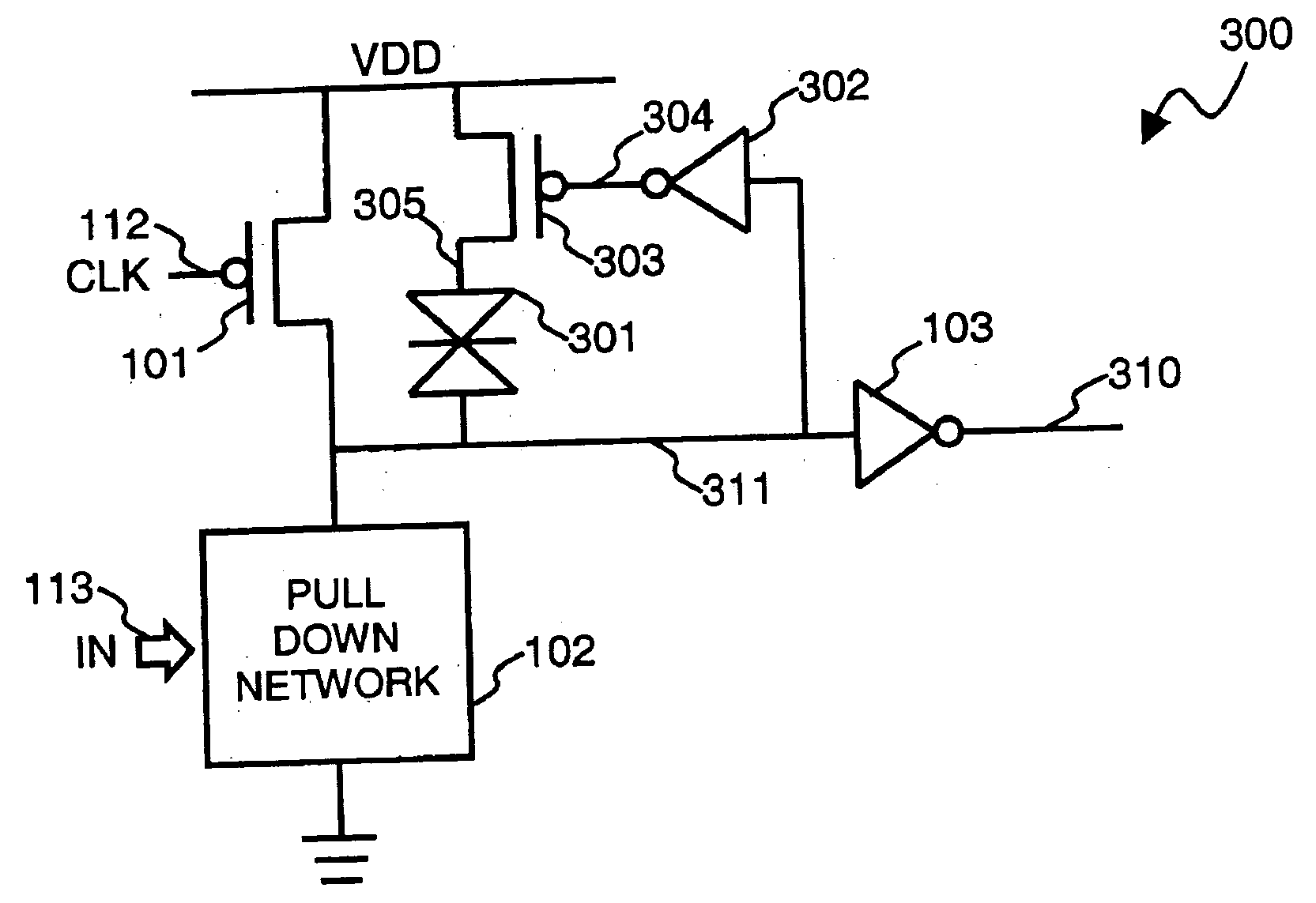
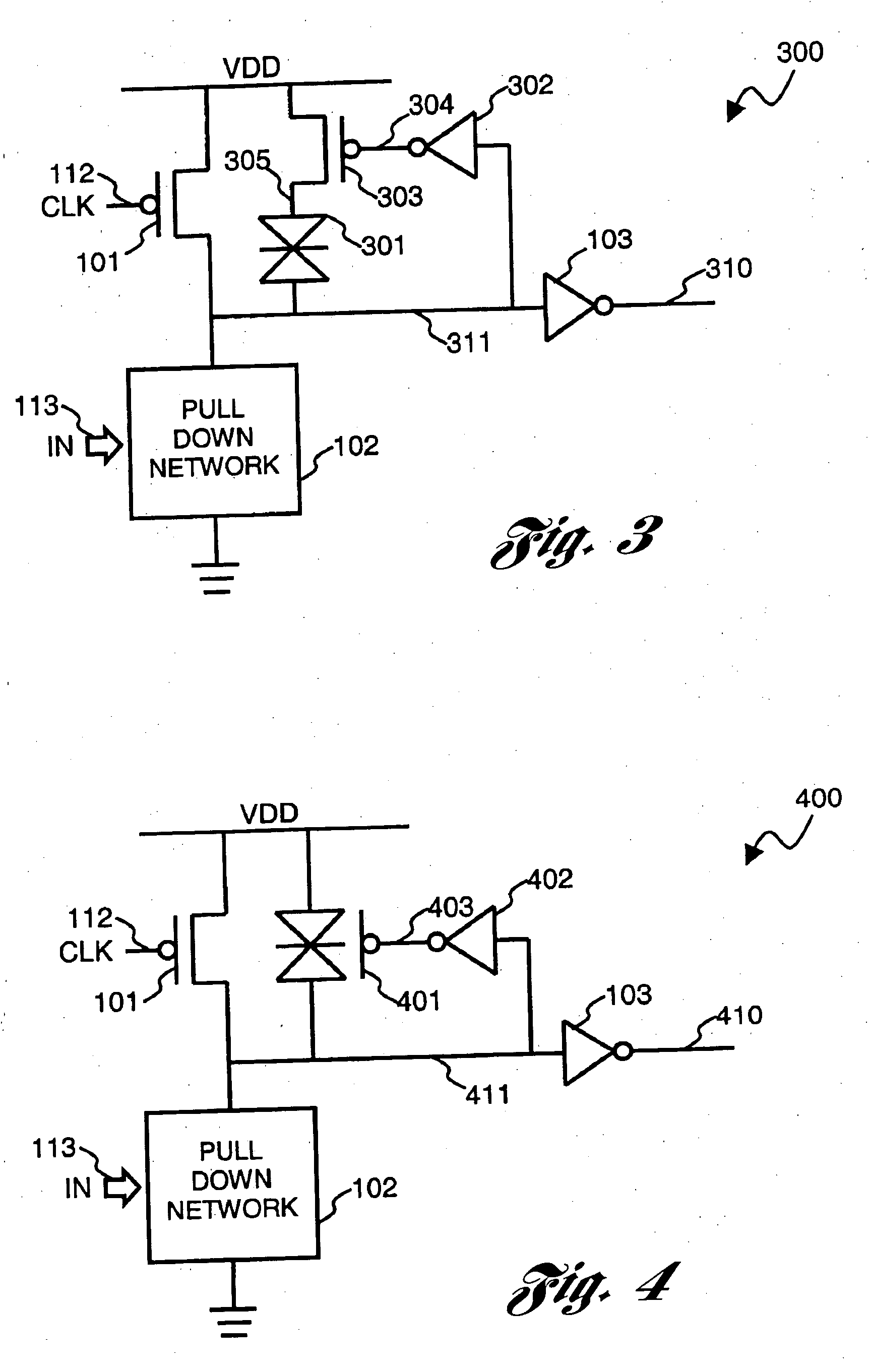
The use of a keeper causes contention when the pull-down network is ON during the evaluation phase, resulting in slower overall gate performance.
However, dynamic gates with those keepers are still susceptible to
external noise glitches because the dynamic node is not adequately protected during the gate
switching time window.
However, there is a fundamental dilemma in choosing the size of the keeper.
On the other hand, large keeper leads to significant contention during normal gate switching operation, and therefore deteriorates gate performance.
In complex dynamic logic gates with a large pull-down network,
charge sharing between the dynamic node and the internal nodes in the pull-down network often results in false gate switching.
Finally, it is noted that techniques based on precharging internal nodes alone are not very effective against external noises.
However, this technique significantly lengthens the
discharge path in the pull-down network, which potentially leads to slower circuit or considerably increased circuit active area when the transistors are aggressively sized.
However, this technique leads to increased gate input
capacitance which may slow down the switching of the gates in the previous stage.
Further, this technique is not suitable for certain logic functions because it may short input nodes.
In addition to the
silicon area overhead associated with the pull-up network, a major drawback of this technique in practice is its ineffectiveness in dealing with very wide logic gates, for example, wide OR gates, where dynamic logic styles really outshine static CMOS logic gates in performance.
The main drawback of this technique is that it is not suitable for OR type logic gates because of possible serious DC currents under certain input combinations.
This gated CMOS
inverter technique does not completely solve the DC conducting problem for certain logic circuits.
While it can be useful for certain logic gates like wide-OR gates, it is not practical to be applied to general pull-down NMOS network because of its overhead in circuit area and performance.
It is shown in the table that the twin
transistor technique and CMOS
inverter based techniques are not suitable for all logic functions.
Techniques based on precharging internal nodes as well as the two new feedback keeper techniques only improve gate
noise immunity against certain types of noises.
Both the PMOS pull-up technique and the NMOS pull-up (with feedback) technique consumes DC power.
Techniques based on raising source voltage usually either have DC
power consumption or require significantly larger
silicon area.
Techniques based on constructing complementary p-network often require larger
silicon area and they increase the previous stage gate
delay due to greater gate input
capacitance.

