Metal precursors for low temperature deposition and methods of forming a metal thin layer and manufacturing a phase-change memory device using the metal precursors

a technology of metal precursors and low temperature deposition, which is applied in the direction of instruments, germanium organic compounds, antimony organic compounds, etc., can solve the problems of preventing the integration of the device, preventing the fine contact of the phase change material layer, and preventing the expansion of the devi

Active Publication Date: 2008-05-08
SAMSUNG ELECTRONICS CO LTD
View PDF5 Cites 39 Cited by
  • Summary
  • Abstract
  • Description
  • Claims
  • Application Information

AI Technical Summary

Benefits of technology

[0009]The present invention provides metal precursors for low temperature deposition. Embodiments of the present invention provide metal precursors for low temperature deposition including a metal ring compound including at least one metal as one of a plurality of elements forming a ring, wherein the metal precursor is suitable for low temperature deposition.
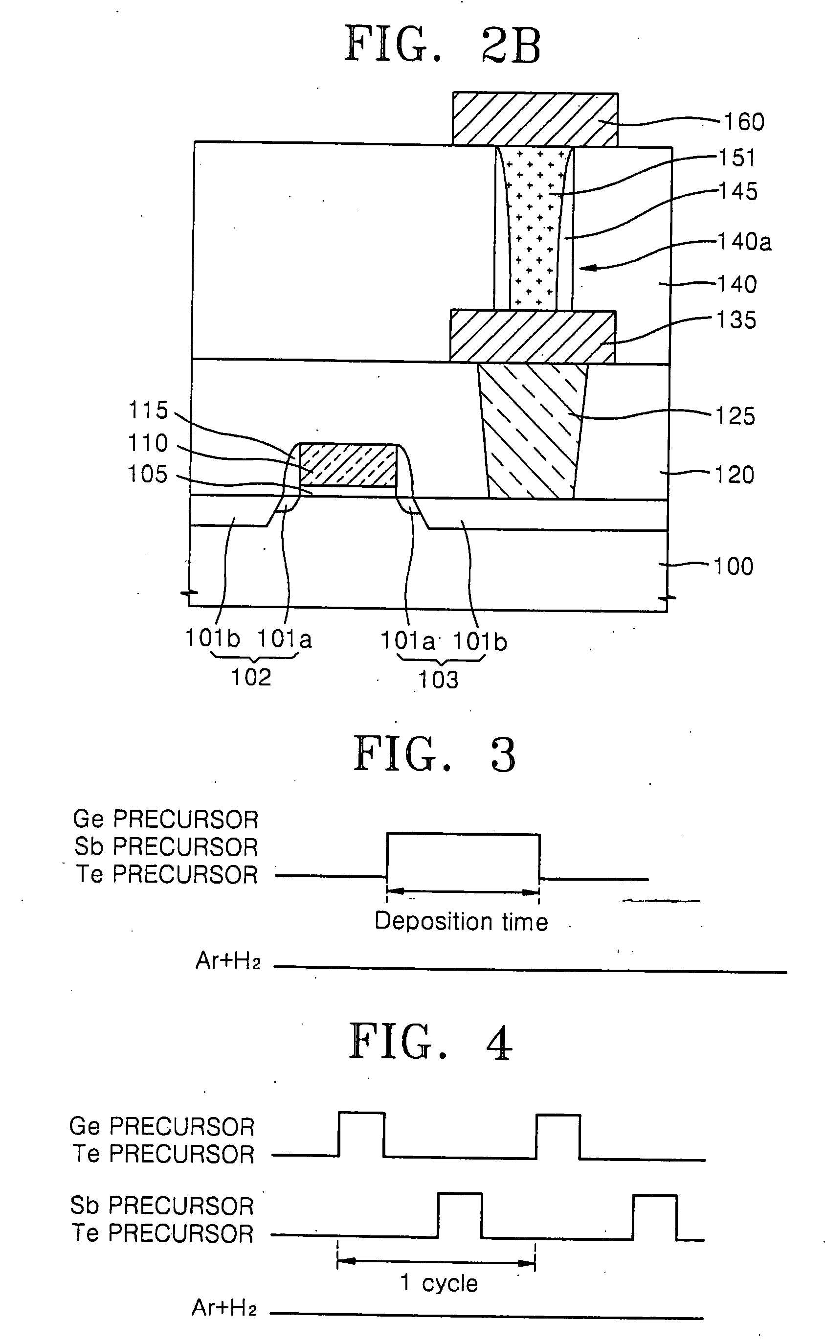
[0010]The present invention also provides methods of forming a metal thin layer using the metal precursors for low temperature deposition. Embodiments of the present invention provide methods of forming a metal thin layer, including supplying to a substrate at least one metal precursor having a metal ring compound, wherein the metal ring compound includes at least one metal as one of a plurality of elements forming a ring, thereby forming a metal thin layer on the substrate.
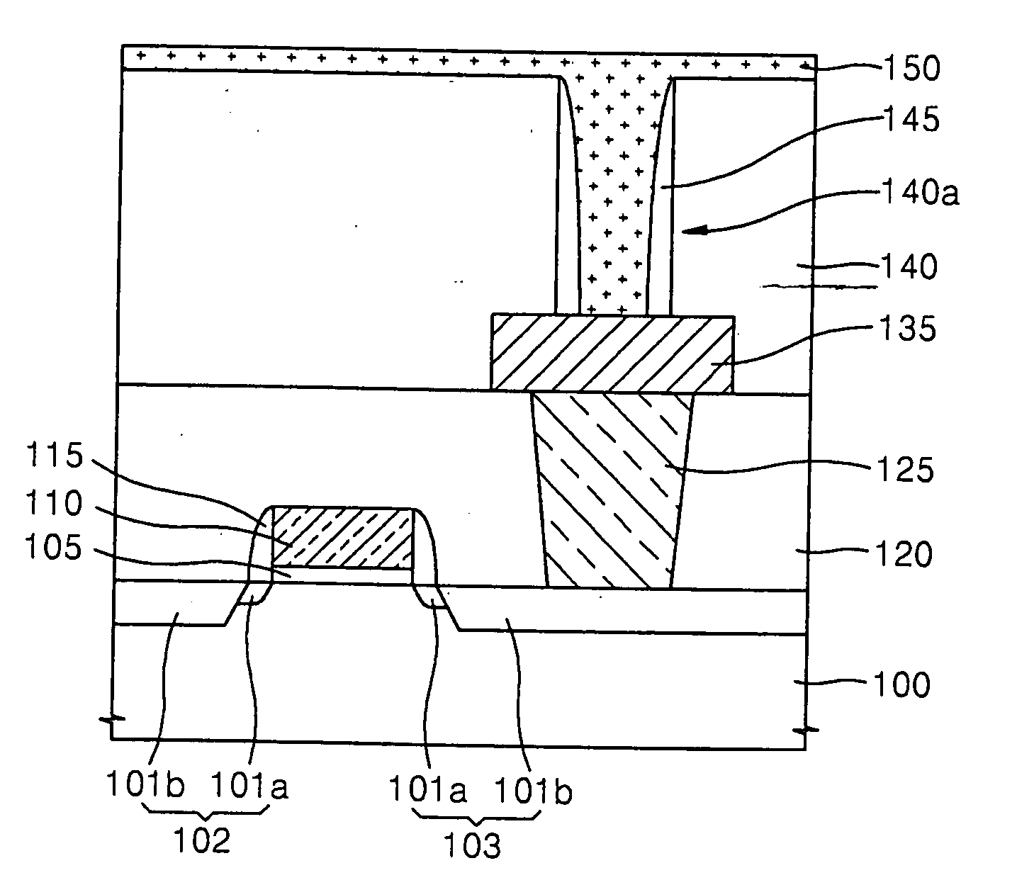
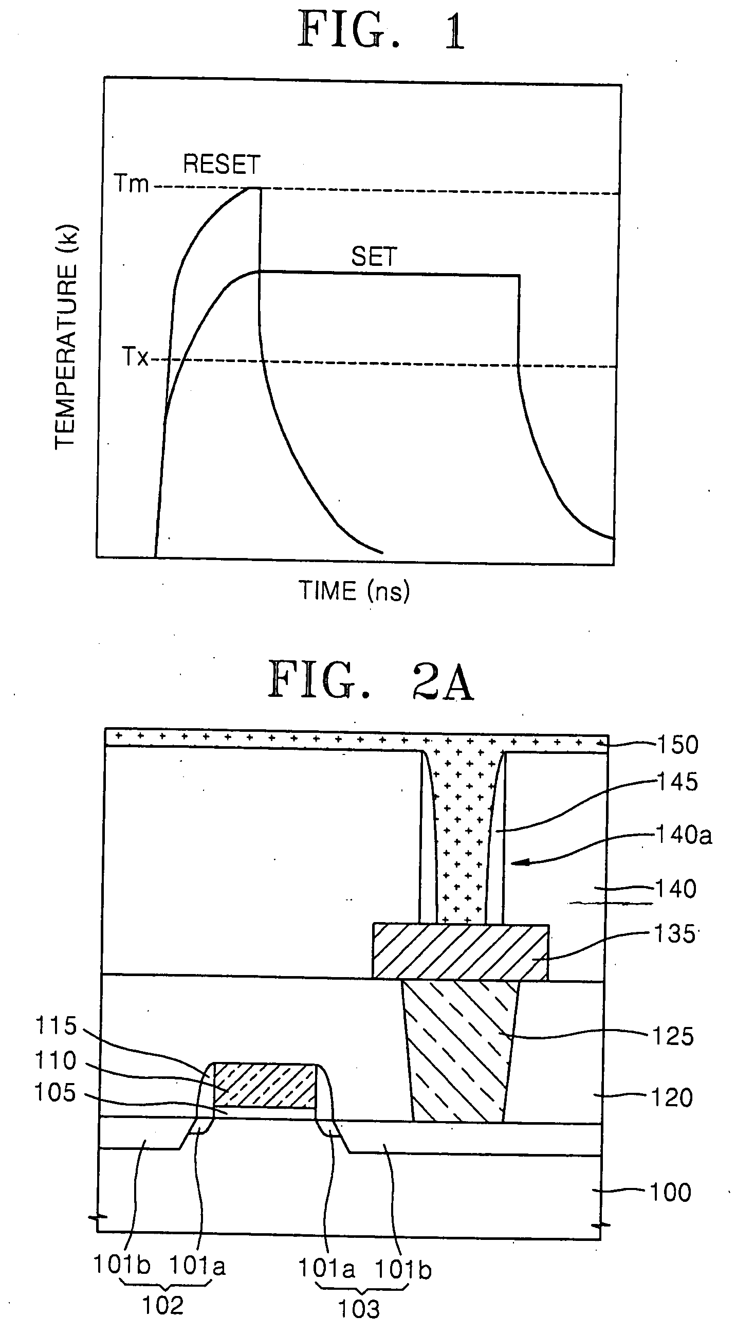
[0011]The present invention also provides methods of manufacturing a phase change memory device, in which fine contact holes can be filled stably, with little to no void formation, using the metal precursor for low temperature deposition. Embodiments of the present invention provide methods of manufacturing a phase change memory device, the methods include: forming a bottom electrode on a substrate; forming a mold insulating layer on the bottom electrode; forming a via hole exposing at least a portion of the bottom electrode in the mold insulating layer; supplying to the substrate to fill the via hole with a phase change material layer a metal precursor including a metal ring compound wherein the metal ring compound including at least one metal as one of a plurality of elements forming a ring; and forming a top electrode on the phase change material layer.

Problems solved by technology

During reset programming, in order to apply a relatively high current, the size of the access device may be enlarged; however, this action can present an obstacle for increasing the device integration.
However, the phase change material layer is typically formed using a sputtering method, and thus, it may be problematic to fill the via holes without voiding at least due to step coverage of the phase change material layer formed using the sputtering method.
However, it is generally problematic to fill fine contact holes with the phase change material layer at least because of the size of grains of the phase change material layer formed at a relatively high temperature of 700° C.

Method used


Image

  • Metal precursors for low temperature deposition and methods of forming a metal thin layer and manufacturing a phase-change memory device using the metal precursors
  • Metal precursors for low temperature deposition and methods of forming a metal thin layer and manufacturing a phase-change memory device using the metal precursors
  • Metal precursors for low temperature deposition and methods of forming a metal thin layer and manufacturing a phase-change memory device using the metal precursors

Examples


synthesis example 1

Synthesis of Ge Ring Compound

[0075]24.31 g of metal magnesium (1000 mmol) was suspended in 500 mL of diethyl ether in a reactor of 2 L. After a water bath was installed in the reactor, 130.7 g (500 mmol) of 1,4-dibromobutane was slowly added to the magnesium diethyl ether suspension. Here, the addition speed of 1,4-dibromobutane was adjusted such that the temperature of the reaction solution was maintained at 25° C. After the addition of 1,4-dibromobutane was completed, the reaction solution was agitated for 3 hours at a room temperature. Then 53.6 g (250 mmol) of germanium tetrachloride (GeCl4), which was diluted in 100 mL of diethylether, was slowly added to the reaction solution and then the reaction solution was agitated for 16 hours at a room temperature and then the reaction was completed. After the reaction was completed, the reaction solution was filtered at a reduced pressure to obtain a colorless filtered solution. The colorless filtered solution was fractionally distilled...

example 1

Examination Example 1

[0076]FIG. 6 presents a graph showing 1H-NMR analysis of the liquid compound manufactured according to the methods described above in Synthesis Example 1. The 1H-NMR analysis was carried out in C6D6, at 25° C. Referring to FIG. 6, a peak at 1.59 ppm denotes a hydrogen (Ge—CH2CH2CH2CH2—) that is bonded to a carbon that is not bonded to Ge in Formula 3, and a peak at 0.83 ppm denotes a hydrogen (Ge—CH2CH2CH2CH2—) that is bonded to carbon that is bonded to Ge in Formula 3. Accordingly, 5-germaspiro[4,4]nonane represented by Formula 3 can be synthesized by the above Synthesis Example 1.

example 2

Examination Example 2

[0077]FIG. 7 presents a graph showing differential thermal analysis (DTA) of the liquid compound, i.e., the Ge ring compound represented by Formula 3, manufactured according to methods described in Synthesis Example 1. Referring to FIG. 7, the Ge ring compound represented by Formula 3 is thermally decomposed at about 200° C., and thus, generates Ge.


PUM

PropertyMeasurementUnit
temperatureaaaaaaaaaa

Abstract

The present invention provides metal precursors for low temperature deposition. The metal precursors include a metal ring compound including at least one metal as one of a plurality of elements forming a ring. Methods of forming a metal thin layer and manufacturing a phase change memory device including use of the metal precursors is also provided.

Description

CROSS-REFERENCE TO RELATED PATENT APPLICATION[0001]This application claims priority under 35 U.S.C. §119 to Korean Patent Application No. 10-2006-0109580, filed on Nov. 7, 2006, the disclosure of which is incorporated by reference herein in its entirety.FIELD OF THE INVENTION[0002]The present invention relates to metal precursors, methods of forming a metal thin layer using the metal precursors, and methods of manufacturing a semiconductor device using the metal precursors.BACKGROUND OF THE INVENTION[0003]A phase change material is a material that changes into a crystalline state or into an amorphous state in response to changes in temperature. The specific resistance of the phase change material in the crystalline state may be lower than that in the amorphous state. This feature of the phase change material may allow the phase change material to be used in a memory device, for example, a phase-change random access memory (PRAM).[0004]A unit cell of a PRAM includes an access device ...

Claims


Application Information

Patent Timeline
Patent Type & Authority Applications(United States)
IPC IPC(8): H01L21/06B32B15/04C07C395/00C07F7/30H01L21/44C07F9/90C23C16/00
CPCC07F7/30C23C16/18C23C16/305H01L27/2436H01L45/1683H01L45/1233H01L45/144H01L45/1616H01L45/06Y10T428/31678H10B63/30H10N70/231H10N70/023H10N70/826H10N70/8828H10N70/066G11C13/0004
Inventor PARK, HYE-YOUNGCHO, SUNG-IAEBAE, BYOUNG-JAELEE, JIN-ILLIM, JI-EUNPARK, YOUNG-LIM
Owner SAMSUNG ELECTRONICS CO LTD
Why Eureka
Try Eureka