Method of forming a protective layer on thin-film photovoltaic articles and articles made with such a layer

a technology of protective layer and thin film, which is applied in the direction of semiconductor/solid-state device manufacturing, semiconductor devices, electrical devices, etc., can solve the problem that the protective layer cannot be formed using standard chemical vapor deposition methods, and achieve good barrier properties and improve resistance to environmental elements

Inactive Publication Date: 2010-09-30
DOW GLOBAL TECH LLC
View PDF16 Cites 29 Cited by
  • Summary
  • Abstract
  • Description
  • Claims
  • Application Information

AI Technical Summary

Benefits of technology

[0007]Surprisingly, the present inventors have discovered that inorganic barrier films (preferably silicon nitride) can be applied to chalcogenide based PV devices at low temperatures to provide good barrier properties. Specifically, the applicants have discovered that chalcogenide cells with improved resistance to environmental elements can be formed by direct low temperature deposition of inorganic barrier layers onto the cell but such layers cannot be formed using standard chemical vapor deposition methods to provide the barrier layer. Moreover, applicants have discovered that a unique multilayer barrier can be formed in a single step when reactive sputtering of the silicon nitride onto an inorganic oxide top layer of the PV device.

Problems solved by technology

Specifically, the applicants have discovered that chalcogenide cells with improved resistance to environmental elements can be formed by direct low temperature deposition of inorganic barrier layers onto the cell but such layers cannot be formed using standard chemical vapor deposition methods to provide the barrier layer.

Method used


Image

  • Method of forming a protective layer on thin-film photovoltaic articles and articles made with such a layer
  • Method of forming a protective layer on thin-film photovoltaic articles and articles made with such a layer
  • Method of forming a protective layer on thin-film photovoltaic articles and articles made with such a layer

Examples


example 1

CIGS Cells

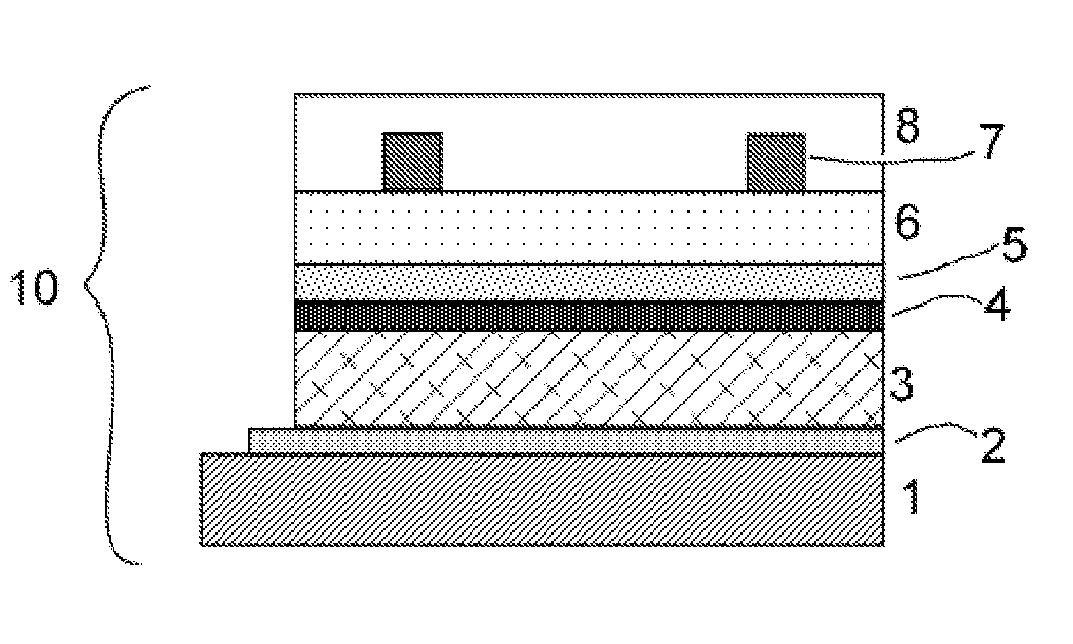
[0030]CIGS-based cells are used which have a substrate of a Fe—Cr, body-centered cubic (BCC) stainless steel. The front side of the substrate is coated with a thin bilayer of chromium (Cr) and molybdenum (Mo) to form the back contact. Next, the absorber layer is fabricated by depositing a thin layer of NaF and then co-evaporating Cu, In, Ga, and Se (CIGS). The cadmium sulfide (CdS) buffer layer is deposited by chemical bath deposition (CBD). A thin, intrinsic ZnO (iZnO) serves as the window layer, which is then capped by an InSnO (ITO) transparent conductive oxide (TCO) layer. The device is completed by screen printing an Ag collection grid on the ITO. The initial cell efficiencies were on average 6.94±0.77%.

Sputtering Method

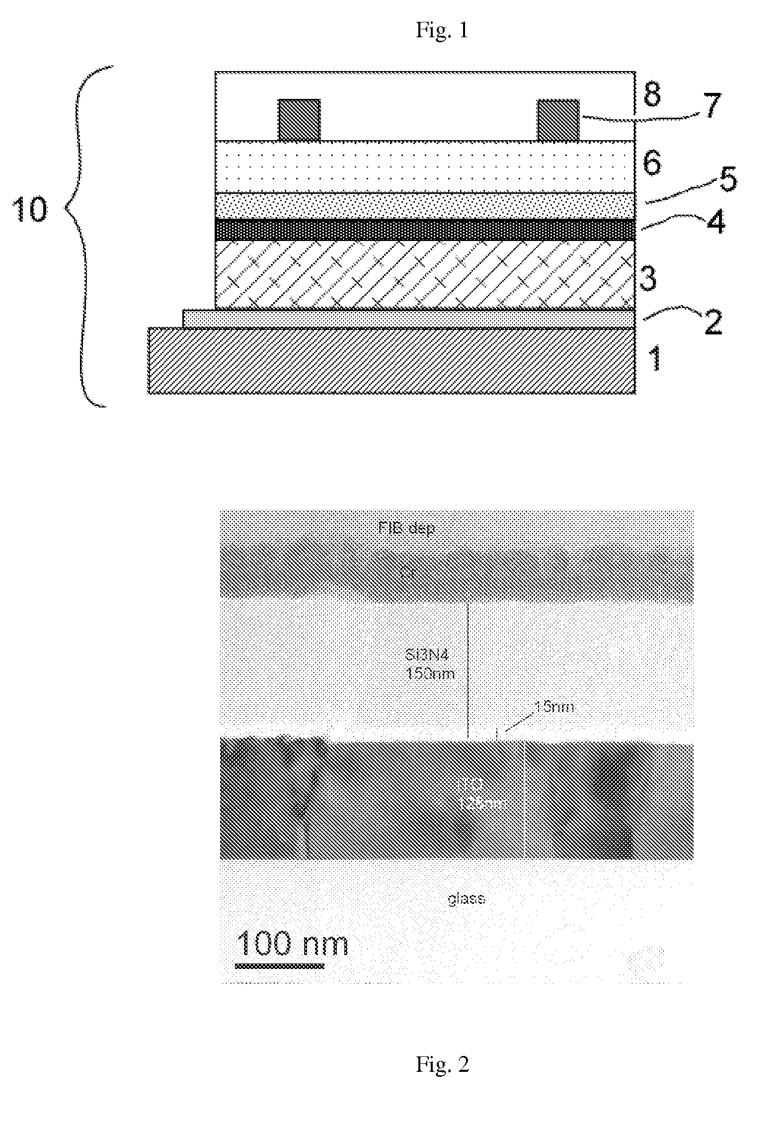
[0031]Silicon nitride films are deposited from a pure Silicon target within an 80:20 Ar / N2 gas mixture. The deposition rate is experimentally determined prior to sample generation for each deposition recipe. This technique ensures the film thickness de...

example 2

[0035]Photovoltaic devices are prepared on 2″ square soda-lime glass substrates, 0.7 mm thick. A layer of molybdenum is sputter deposited at 200 W, 6e10−3 mbar on the glass substrate, to a final thickness of about 750-800 nm. CIGS absorber layer is deposited by a multi-stage metal co-evaporation process based on a three stage process practiced by National Renewable Energy Laboratory (NREL) (Repins, 2008). A cadmium sulfide buffer layer is deposited by chemical bath deposition (CBD) by dipping samples into a mixture of 33 mL 0.015 M CdSO4(aq) and 42 mL 14.5 M NH4OH(aq) (concentrated NH3) at 70° C. After 1 min 33 mL of 0.75 mL thiourea is added and the reaction is allowed to proceed for 7 min Samples are dried at 110° C. for 30 min The window layer, i-ZnO, is prepared by RF magnetron sputtering of a ZnO target at 60 W and 10 mtorr sputtering pressure (0.15% O2 in Ar sputtering gas) to a final thickness of about 70 nm. Indium tin oxide (ITO) films are prepared using a custom RF magnetr...

example 3

[0036]CIGS-based devices, with and without nitride encapsulation made substantially as set forth in Example 1, are subjected to damp-heat, 85° C. / 85% RH, environmental weathering conditions as specified in IEC standard 61646. During the exposure, the cells are positioned vertically on a stainless steel fixture situated above a pool of DI water within a lab oven held at 85±5° C. To mitigate premature failure due to moisture ingress from the device edge, the devices are clamped in a metal or glass based package—we refer to this as the “packaged device”. Furthermore, a layer of silicone grease is applied to the edge of each device to reduce the likelihood of a cell experiencing premature failure due to moisture-ingress at the device edge. Periodically during the experiment the cells are removed from the test environment, and their package, and their I-V characteristic is measured. Prior to collecting the I-V characteristic measurement, the samples rest in a dry nitrogen purged box for ...


PUM

PropertyMeasurementUnit
temperaturesaaaaaaaaaa
temperatureaaaaaaaaaa

Abstract

Chalcogenide based photovoltaic devices cells with good resistance to environmental elements can be formed by direct low temperature deposition of inorganic barrier layers onto the film. A unique multilayer barrier can be formed in a single step when reactive sputtering of the silicon nitride onto an inorganic oxide top layer of the PV device.

Description

CROSS-REFERENCE TO RELATED APPLICATION(S)[0001]This application claims benefit of priority from U.S. Provisional Patent Application No. 61 / 163,101, filed Mar. 25, 2009, which application is incorporated by reference herein in its entirety.FIELD OF THE INVENTION[0002]The invention disclosed herein relates generally to the field of thin-film photovoltaics and methods of forming protective layers on such photovoltaic devices.BACKGROUND OF THE INVENTION[0003]Non-polluting sources of energy are actively being sought as a replacement for the burning of fossil fuels. The generation of energy from solar radiation is one type of clean energy that is receiving significant attention. Solar energy collectors, such as photovoltaic cells (also referred to as “solar cells”), may be used to generate energy where and when there is adequate sunlight. While silicon based solar cells are prevalent, they suffer from certain disadvantages. For example, the silicon based solar panels tend to be relatively...

Claims


Application Information

Patent Timeline
Patent Type & Authority Applications(United States)
IPC IPC(8): H01L31/0216H01L31/18
CPCH01L31/02167Y02E10/50H01L31/0749H01L31/048H01L31/0445Y02E10/541
Inventor DEGROOT, MARTY W.FEIST, REBEKAH K.BERNIUS, MARK T.BANHOLZER, WILLIAM F.YEUNG, CHUNG-HEISREERAM, ATTIGANAL N.HALEY, JR., ROBERT P.
Owner DOW GLOBAL TECH LLC
Why Eureka
Try Eureka